By Peter J Mayhew
A dissertation submitted in partial fulfilment of the requirement of the University of the West of England, Bristol for the Degree of Master of Science
November 2011
Revision History
Rev Sections Affected Remarks
Issue 1 All Author: P. Mayhew
Date: 23/11/2011
Abstract
One of the growing concerns in avionics is Single Event Effects which can cause temporary data corruption on sensitive devices, such as FPGAs. Without mitigation, Single Event Upsets can cause undesirable effects, or worse catastrophic failure on avionic systems. This is especially the case at higher altitudes.
Several mitigation techniques are reviewed with evidence to suggest that combining multiple mitigation techniques such as TMR and memory scrubbing results in a system which is almost immune to Single Event Upset failure.
This dissertation presents research on Embryonic’s (Embryological Electronics) by studying the biological defence mechanisms of Eukaryote cells. The aim of this report is to develop a biologically inspired behavioural model in VHDL which can tolerate Single Event Upsets.
The behavioural model uses a cluster of embryonic cells in a cellular array which are configured by reading a configuration table (Genome). The Genome defines the functionality, timing, data path routing for each embryonic cell.
The study finds that the Genome successfully configures the cluster of embryonic cells to perform the function of a half adder. Using partial reconfiguration the cluster demonstrates fault tolerance against Single Event Upset.
Acknowledgements
University of the West of England
Frenchay Campus
Coldharbour Lane
Bristol
BS16 1QY

Supervisor: Nigel Gunton
Secondary Supervisor: Gabriel Dragffy
Introduction
Background
Aircraft systems are subjected to a wide range of environmental influences during their in-flight service. Therefore, before a system can be used for commercial or military flight a qualification unit is tested to an agreed specification by the stakeholders. This validates the unit can withstand agreed environments conditions. Typically, the types of tests performed on a qualification unit include, thermal, vibration, electromagnetic emission and electromagnetic susceptibility, lightning etc.
One of the growing concerns in avionics is the susceptibility of Single Event Effects (SEE) which impacts both the reliability and the safety of avionic equipment. Single event effects can cause temporary data corruption on sensitive devices such as Field Programmable Gate Array (FPGA) which if not mitigated can cause an avionics unit to produce undesirable effects, or worse catastrophic failure. Single Event Effects failures are difficult to diagnose since they only produce a temporary failure. Therefore, customer returned units may pass all tests and the technician may report no fault found. This is not desirable, as early life returns not only increases warranty costs, but also tarnishes the customer relationship. The purpose of this report is to research the effects of ionising radiation on aviation systems during flight. Also to review suitable mitigation techniques which can reduce the risks associated with single event effects and therefore improve flight safety and maintainability.
Product Justification
A customer requires a small displays navigation unit before the 2nd quarter of 2012. Deliverable must demonstrate fault tolerance against simulated ionised radiation.
Project deliverables
The project deliverables shall be defined by a high level Work Breakdown Structure (WBS). This defines the work and processes involved to execute this project, develop the project schedule. The WBS would normally show the resource requirements and costs, but this is out of scope for this project.
Figure ‑ Work Breakdown Structure
Project Aims and Objectives
The aim of this report is to develop a biologically inspired behavioural model in VHDL which can tolerate Single Event Effects.
The primary objectives are:
- Research ionised radiation. Discuss the reasons why this can impact the flight safety of avionic systems.
- Review and evaluate mitigation techniques to improve the system reliability against Single Event Upsets.
- Research Eukaryote and Prokaryote cells. Discuss the biological defence mechanisms.
- Design, develop, and synthesise a biologically inspired behavioural model in VHDL.
- Verify the biologically inspired behavioural model can configure as a half adder. Validate the functional correctness.
- Repeat objective 5 with a Single Event Effect. Verify the biologically inspired behavioural model reconfigures. Validate the functional correctness.
Project Planning Assumptions
- The project shall demonstrate fault tolerance by using a biologically inspired approach
- A VHDL behavioural model shall be produced as part of the project
- The project can be simulated, and no practical demonstration required
- Project shall start June 2010 and end November 2011
- Built-in self-test is considered out of scope for this project
- There is no access to a particle accelerator to generate ionised radiation. (Which would demonstrate the robustness of the design)
Constraints
Only 1x demonstration board available at the start of the project which uses the EP20K200EFC484-2X FPGA.
Quartus II web edition software package (Free software package)
Risk Analysis and Compliance
The risk analysis matrix and Compliance matrix, shown in Table 1‑1, is a scorecard that assess some of the potential risks in this project. Mitigation techniques explain how the risks will be avoided and the contingency plan can be used if the risk becomes un-avoidable. (10 high risk, 1 low risk)
|
Risk |
Probability/ Impact Score |
Mitigation |
Contingency |
Impact |
|
Minimal experience on biology. No experience on biological defense mechanisms |
7 |
Review other research papers and media to understand how biological cells work and their defense mechanisms |
Research only the required information on biological defense mechanisms |
Failure to understand and adopt a biological defense mechanism which could be implemented into a behavioral model. |
|
Simulated design may not function as expected |
9 |
Use a modular approach. Test and verify each part before merging into overall design |
Document that the design did not function as expected. Suggest an alternative method for future work |
Failure to demonstrate functionality of design |
|
Design may not prove to be fault tolerant |
6 |
Review more than 1 fault tolerance technique. Allow sufficient time review and compare solutions before implementing 1 into final design. |
Document that the design did not function as expected. Suggest an alternative method for future work |
Failure to demonstrate effectiveness of fault tolerance using the design |
|
Learning curve associated with tools to develop VHDL |
5 |
Allow sufficient time to develop the VHDL. Start early in the project |
Add process reengineering and additional CRP time to schedule |
Risk of delaying development and not reaching some milestones |
Table ‑ Risk Analysis And Compliance Matrix
Document overview
Section 2 : Overview of ionised radiation. How this impacts avionic equipment.
Section 3 : Reviews some of the common FPGA mitigation techniques used in industry.
Section 4 : Reviews biological cells to understand their defence mechanism.
Section 5: Design mythology for the embryonic VHDL behavioural model.
Section 6 : Verification tests performed on the embryonic cells.
Section 7 : Simulation and verification tests performed on the embryonic cells.
Section 8 : Conclusions which provide a discussion on the project outcomes, achievements, weaknesses, recommendations, future research, and personal reflection.
Appendix A : Project plan.
Appendix B : Supplementary Avionics Research.
Appendix C : Supplementary Biologic research including a breakdown of the eukaryote cells
Appendix D : Supplementary Systems Research including original VHDL designs, SEE types, Error detection techniques.
Appendix E Supplementary testing performed on the Embryonic Cells.
Appendix F : Circuit Diagrams for the Embryonic Cells.
Appendix G : Flow Charts for the Embryonic Cells.
Appendix H : VHDL for the Embryonic Cell
Glossary
Ionizing Radiation: Any radiation, as a stream of alpha particles or x-rays that has sufficient energy to detach electrons from atoms or molecules.
Gray (Gy): The unit of radiation dose in the SI system. One Gy represents the absorption of 1
joule ( J) of energy by 1 kg of any material.
Sievert (Sv): The unit of radiation dose equivalent in the SI system.
Radiation dose: A way of describing the amount of energy transferred into a material that has been exposed to radiation. The unit of radiation dose in the SI system is the gray (Gy).
Rem: (obsolete): Equivalent dose is dimensionally a quantity of energy per unit of mass, and is usually measured in sieverts or rems.
Cosmic Radiation: The ionizing radiation that originates outside the solar system, a main source of which is thought to be exploding stars (supernovae).
Single Event Effect: Events caused by a single charged particle such as heavy ions or protons.
Prokaryote: An organism characterised by the absence of a nuclear membrane and by DNA that is not organized into chromosomes.
Eukaryote: A single-celled or multicellular organism whose cells contain a distinct membrane-bound nucleus.
Ionised Radiation and Flight Safety
The purpose of this section is to develop the readers understanding on ionised radiation which is followed by discussing the relationship between ionised radiation versus altitude.
Next, the impact of ionised radiation on electronics shall be reviewed which explains why Single Event Effects is a concern in the avionics industry. Finally, we shall review some of the mitigation techniques used in industry and how this impacts the systems reliability.
Ionised Radiation
Since the start of the 20th century there has been significant interest amongst the scientific community; to the unknown origin of radioactivity. This includes ionised radiation which was measured in all parts of the globe. It was the work of Professor Victor Hess who found that ionised radiation levels increased in proportion with altitude. Hess’s investigations showed that at 9,300m the radiation level were 40 times more intensive than on the earth’s surface (1) (2).
Natural occurring radiation has a number of sources such as cosmic rays from outside our solar system, charged particles from our Sun in solar winds and the radioactive decay of materials found in the earth’s environment (3). Since solar activity cycles about every eleven years it is possible for avionic systems to be exposed to an increased level of ionised radiation for duration of a couple of hours (4) (5). The reader might ask why not service the plane every ten-eleven years to coincide with this. One of the problems with ionised radiation is that some effects are accumulative and others are temporary.

Figure ‑ Sunspot Observations cycles every 11 years (5)
Ionised radiation is radiation which has sufficient energy to detach electrons from atoms or molecules and is found in the form of alpha particles, beta particles, gamma rays and x-rays, as shown in Figure 2‑2. Alpha particles (α) are positively charged and due to their large molecules and can be stopped by paper or skin. Beta particles () are electrons which can penetrate deeper than alpha particles, but can still be stopped by a thick layer of metal or water. Gamma rays (γ) and x-rays are known as electromagnetic radiation and can penetrate much further, even into lead and concrete (6).
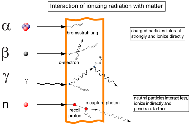
Figure ‑ Types of Radiation (6)
In recent years there has been significant research by the World Health Organisation on the amount of atmospheric radiation the passengers and crew are exposed to during flight. One of the World Health Organisation programmes is The Radiation and Environmental Health Programme and this evaluates the health risk and public health issues in relation to occupational radiation exposure (7). The Federal Aviation Administration (FAA) Civil Aerospace Medical Institute have developed a system which gathers data from the Space Environment Services Centre of the National Oceanic and Atmospheric Administration (NOAA) which provides alerts on any disturbances on the Sun which could results in a high dose-rate of ionised radiation being subjected to the Earth’s atmosphere. Pilots respond to this alert by reducing the aircrafts altitude, and hence reduce radiation exposure (8). The FAA published the effective dose rates on aircraft from solar radiation is 30,000-60,000ft as shown in Figure 2‑3. This verifies that aircraft flying at higher altitude receive a higher effective dose rate of ionised radiation and therefore confirms the validity of Hess’s research.
Figure ‑ Effective dose rates from solar ionizing radiation at three altitudes on 20th January 2005 (9)
The research conducted by British Airways gives a reasonable indication of the ionised radiation levels present whilst their aircraft is in flight and is shown below in Table 2‑1.
|
Type of British Airways Aircraft |
Microsieverts per hour |
|
Concorde |
12-15 µSv |
|
Long haul aircraft |
5 µSv |
|
Short haul aircraft |
1-3 µSv [1] |
Table ‑ Measured Ionised Radiation Levels by British Airways (10)
Data collected from The World Health Organisation shows the estimated amount of radiation measured during flight, and is shown in Table 2‑2. The table has been expanded by calculating the microSievert per hour. This was achieved by divided the estimated radiation dose by the duration (hours).
|
Cosmic radiation dose on selected flights[2] |
|||||
|
Flight |
|||||
|
From |
To |
|
Duration (hours) |
Estimated Radiation dose (microSievert) |
Estimated microSievert / hour |
|
Sydney |
Singapore |
7.50 |
17 |
2.26 |
|
|
Bangkok |
Washington |
28.10 |
70 |
2.5 |
|
|
London |
Tokyo |
12.00 |
58 |
4.8 |
|
|
Buenos Aires |
Athens |
18.35 |
41 |
2.24 |
|
|
New York |
Paris |
7.00 |
35 |
5 |
|
|
Frankfurt |
Los Angeles |
9.50 |
51 |
5.36 |
|
|
Johannesburg |
Mumbai |
9.10 |
16 |
1.7 |
|
Table ‑ Cosmic radiation dose on selected flights [23]
Using the estimated radiation dose from Table 2‑2 we can calculate the arithmetic mean microSievert as shown in Equation 1.
Equation Average cosmic radiation reading by The World Health Organisation
The arithmetic mean was also taken from the British Airways results in Table 2‑1, and this has been calculated in Equation 2.
Equation Average cosmic radiation reading by British Airways
Based on this research, it would be reasonable to expect a reading between 3.41-6.66µ Sievert on average during flight. Whilst these results are useful, the reader might question why the results from two independent investigations differ. Upon further review, the author found the data from the World Health Organization had based its readings on “…cruise altitude of 10.000 m”; which equates to 32,000ft. However, Concord fly’s at 60,000ft. This would account for the radiation levels with British Airways being higher.
It is the same atmospheric radiation exposure on the aircrafts & crew effects can contribute to hard and soft faults in aviation equipment which commonly known as Single Event Effects (11).
Effects on Electronics
As a result of SEU, additional tests are required for commercial aircraft, military aircraft, and spacecraft to reduce the probability of failure. This is because a system failure on avionic equipment could result in the loss of human life or catastrophe. This can also result in high costs such as spacecraft which are very difficult to repair at long distances.
During take-off, the aircraft is travelling at low altitudes, so the electronics are less likely to be affected by the ionised radiation. Light aircraft and helicopters are less susceptible to the ionised radiation compared to commercial and military aircraft which generally fly at higher altitudes (12).
Electronics has been used in space exploration since the 1960’s and it was understood that the electronics needed to survive a much greater level of ionised radiation than equipment on the ground. Therefore, the electronics used space exploration applications were assessed for ionised radiation susceptibility and guidelines for their use developed (2).
During the 1970’s electronics were being used in safety critical functions on aircraft. Generally the components used were of military grade or internationally approved as this gave an independent assessment. However, in the latter years it became common practice for commercial parts to be used. As technology advanced, the complexity and lithography techniques resulted in higher IC density. During this time, it was not fully understood how these technological advances would also be a contributing factor to SEU susceptibility.
The research of SEU impacting aircraft was evolving from anecdotal incidents which had little scientific basis. Therefore, during 1988 and 1989 IBM flew a number of flight experiments using three aircrafts travelling over Seattle, Northern California, and Norway. Each aircraft was installed with a large array of 64k Static Random Access Memories (SRAM) and the number of SEEs on the SRAM was monitored. Later, IBM and Boeing were sponsored for a study by the Defence Nuclear Agency and Naval Research Laboratory. They used the data previously collected by IBM and the SEU’s monitored in a CC-2E flight computer on TS-3 E-3 military aircraft which flew mainly over West Coast. This study was completed in 1992 and demonstrated that SEUs in avionics was a scientific fact and that the in-flight failure rates correlated with the atmospheric neutron flux. These results also showed that the upset rates could be calculated using laboratory SEU data (13) (14).
By the 1990’s the geometric size of the silicon components had been significantly reduced. Some components were at risk of state change or damage since the induced charge from ionised radiation could exceed the critical charge of the component (2). As the manufactures used increasing amounts of memory per system it became an important factor for avionics to determine the SEE rate trends (15). It was during the 1990’s the first occurrence of SEU was observed and documented in avionics (2).
During 2000 the International Electrotechnical Commission (IEC) committee was formed as a worldwide organisation for standardisation comprising all national electrotechnical committees. The IEC published the Process management for avionics – Atmospheric radiation effects TS 62239 which was in circulation from 2003-2005 and then replaced with TS 62396-1 which is still used today.
Atmospheric Radiation Effects
FPGA’s are frequently used in avionic systems since they offer simplicity and flexibility during design. YANMEI (16) reports that the ability to improve a FPGA design avoids high non-recurring engineering costs. However, what YANMEI (16) fails to recognise is the extensive system testing and certification costs required for EASA or FAA approval[3]. Without this flight certification, the modification is not permitted to be used in airborne equipment.
The interactions of ionised radiation with solid state devices such as FPGAs can cause ionisation in the semiconductor and create leakage current paths (17). If an ionised radiation particle collides with a CMOS device, the point of impact can potentially cause a transient change as shown in Figure 2‑4. The effect would depend on the function for that part of the circuit. For example, a memory cell could experience loss of information, which could lead to a system failure (18). Depending on the amount of ionised radiation, we could expect either permanent damage to the semiconductor, or momentary corruption of data.
The radiation effects on electronics can be categorised as either Lattice Displacement or Single Event Effect.
Lattice displacement
Lattice displacement is where the arrangement of the atoms in the crystal lattice is altered, and this can be caused by protons, neutrons, alpha particles, heavy ions and very high energy gamma photons (19). This damage is not temporary, as the crystal lattice, and hence the physical properties of the device are altered. This type of failure can be tolerated by using a FPGA which has radiation shielding. Dose-Depth curves can indicate the ‘stopping power’ or Bremsstrahlung of a variety of material thicknesses. Using this knowledge in combination with the FPGA radiation sensitivity will allow the engineer to develop a circuit which can tolerate its intended environment. The use of excessive shielding will increase the aircrafts weight. Therefore, the aircraft infrastructure should be assessed to determine which sensitive areas require radiation shielding. Studies have shown that whilst shielding is beneficial and reduces hazard caused by radiation, in some cases large thickness of shielding can worsen the effects. A heavy ion for example passing through though a certain thickness of material is slowed down to such an extent that its linear energy transfer and therefore its ability to produce ionisation are increased (20). The amount of ionising radiation on a medium is measured by Total Ionizing Dose (TID). This is the cumulative damage of the semiconductor lattice caused by ionising radiation over a period of time. The TID of the aircrafts life span should therefore be below the threshold of the weakest commercial device.
Figure ‑ Effect of a Charged Particle on a Semiconductor (3)
Single Event Effect
Single Event Effects (SEE) are events caused by a single charged particle such as heavy ions or protons impacting electronics. Shielding has minimal effect since the Beta and Gamma rays can still penetrate material as explained in paragraph 2.1 . SEE includes any measurable effect on a circuit due to an ionised particle strike. There are many forms of SEE such as:
- Single Event Upsets
- Multiple Bit Upset
- Single Event Functional Interrupt
- Single Event Latch-up
- Single Event Transient
- Single Hard Error
- Single Event Burnout
- Single Event Gate Rupture
This report will focus on discussing Single Event Upsets (SEU). However, the reader may read about additional types of SEE in Appendix D.3. SEU is a change of state caused by a high energy particle. For digital circuits this can result in a bit flip, such as changing Logic 0 to logic 1, or vice versa. A SEU does not directly cause the device to fail (hard error). Therefore, it is considered a soft error. This type of failure can be corrected with suitable error detection and correction (4). A system reset, or rewriting the memory data would also restore the device to a functional state.
The SEE failure rate of a component can be determined by the following equation (21)
λ = φ.σ
Equation
Where
λ = SEE Failure Rate (failures per device hour)
φ = Atmospheric Neutron Flux (n/cm2/hr)
σ = Device SEE Cross Section (cm2/device)
The neutral flux is standardised at a conservative 6000 n/cm2/hr which is derived from the typical conditions at 40,000 ft, 45° latitude and particle energies greater than 10MeV. This can be scaled for a given application (21).
Discussion
This section has discussed the relationship between ionised radiation and how it increases with altitude. The secondary research taken from British Airways and the World Health Organisation has also confirmed this relationship. This section has also explained the effects of ionised radiation on electronics which could be used on aviation equipment and completes objective 1 of this report
FPGA Mitigation Techniques
Aircraft electronics are subjected to a wide range of environments conditions such as thermal, vibration, radiation[4], lightning, fluid etc. Therefore, before any units can be certified for flight, they must pass qualification tests. This validates whether the product meets the stakeholders requirements.
Brogley (3) reports that radiation impact is often overlooked. This might have been the case for some organisations historically. However, there are now very tight guidelines for before equipment is certified for flight. Based on industrial experience, the author can confirm that ionised radiation testing is performed and there are procedural guidelines in place.
Traditional, vastly accelerated testing methods are used in industry for ionised radiation susceptibility such as
- Bombarding operating FPGA’s with Hess spectrum neutrons and high energy protons
- Los Alamos Neutron Science Centre (LANSCE) facility (http://lansce.lanl.gov ) and Crocker Labs http://crocker.ucdavis.edu/Site/
Ziegler (22) reports that the life testing of the FPGAs is slow process involving a tester which contains hundreds of chips and evaluating their failure rate costing about $300K / chip.
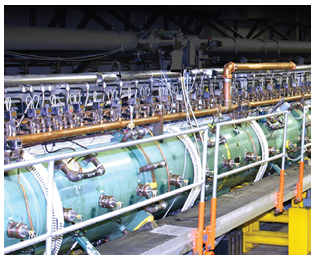 Another approach by Bargg (12) is to use the LANSCE facility to stimulate the effects of atmospheric radiation. This facility uses an 800-mega-electron-volt (800Mev) proton linear accelerator which provides beam current (23). Whilst Bargg (12) reports this is relatively in-expensive, he makes no claims of the costs involved. The rational for this difference in opinion between Ziegler and Bargg would be dependent on the size of the organisation, available budget and the type of testing required.
Figure ‑ LANSCE Linear Accelerator (23)
 The author Ziegler (22) is quoted to say “Life testing at nominal conditions is very frustrating. For example, assume a tester which holds 500 chips which have an estimated SER of about 5000×10-9 fails/hr. This is a typical modern SRAM fail rate per chip. In order to get 50% reliability at two-sigma, you will need to wait for 16 fails or about 9 months. This means that the SER results will not be available until about a year after the first chips start coming out of the fabrication line.”
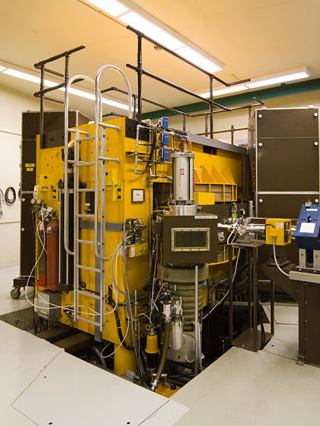
This type of testing is an empirically estimated approach using a Cyclotron which is a type of particle accelerator that uses high frequency AC. It should be noted this can only give us the statistical probability of SEE failure. An example of a Cyclotron is shown in Figure 3‑2.
However, this type of verification is outside the scope of this project. Therefore, a simulated test shall be performed for this report.
As previously discussed in paragraph 2.1 shielding has minimal effect on preventing ionised radiation. Even if a shield was used, it is reported by Ames (25) that it takes several feet of lead to block neutron radiation and this would be far too heavy to load on an aircraft. Also Bargh (12) reports that shielding is impractical as it takes around 3 meters of concrete to reduce neutron influence by 100 times. Since it is impractical to block the radiation other mitigation techniques will need to be explored.
This section shall discus some typical mitigation techniques used in industry to improve the reliability of FPGA’s used in avionic applications. We shall first review three methods to store data on FPGA’s and how they impact the robustness against SEU.
A typical situation for a manufacturer is a product improvement or a design fix which may result in a change to the FPGA firmware. This would typically be identified as a unit part number change for tractability and quality assurance. This allows a system to be reprogrammed without disassembly, reducing direct costs such as labour and preventing human error which could otherwise occur during disassembly / assembly of a unit. Bradley (26) states that the development and qualification costs of safety critical certified hardware is very expensive. However, with careful project management and planning the hardware can be re-used in other designs using a Qualification By Similarity report.
The Qualification By Similarity report is a way to justify to the customer that the hardware does not need to be re-qualified. For example the part might have already been qualified in a different project. Providing the customer agrees with the Qualification By Similarity report, a significant cost and time saving can be made.
Manufactures typically use one of three methods to store their programming data on the FPGA (27).
- Fuses or Antifuses: These FPGAs can be programmed once and use a high voltage to break, or make a connection between logical elements. These devices have high immunity to SEU in their configuration memory. However, because the registers and internal logic are not immune to SEU, the FPGA still requires fault tolerance in its logic design.
- EEPROM: These FPGAs use Electrically Erasable Programmable Read Only Memory EEPROM. As with the Antifuses, these FPGAs also suffer similarly with SEU.
- SRAM base FPGAs: Stores its configuration memory through Static RAM storage cells, which is susceptible to SEU.
Historically antifuse FPGA was used in appose to SRAM based FPGA because the logic is determined by antifuses which are considered to be relatively immune to SEU. However, SRAM based FPGAs have been of significant interest for aerospace electronic systems because they are reprogrammable (16).
SRAM based FPGAs have also gained huge popularity since they can be manufactured using cutting-edge fabrication technologies. This provides high logic gate density & low cost (27). These devices store their configuration data in the SRAM which is susceptible to SEU. If an ionised particle hits the surface of the SRAM within the FPGA there is a risk of bit flipping in the configuration memory from a logic 1 to a logic 0, or vice versa. This is known as a soft error in the industry and is not classed as permanent damage. (2) (16) (28). Normal behaviour can typically be restored by restarting the unit / over-writing the corrupted memory cells. If the radiation changes the configuration data stored in the SRAM cells, this could cause a AND gate being changed to a NAND gate for example. The original designed behaviour of the FPGA would therefore be changed (29), resulting in the incorrect outputs or for the unit to operate unexpectedly.
Effects such as latch-up can cause high operating currents of power transistors. This can result in degraded performance or destructive damage resulting in a potential system failure if not corrected. This is known as a hard error and this is illustrated in Figure 3‑3.
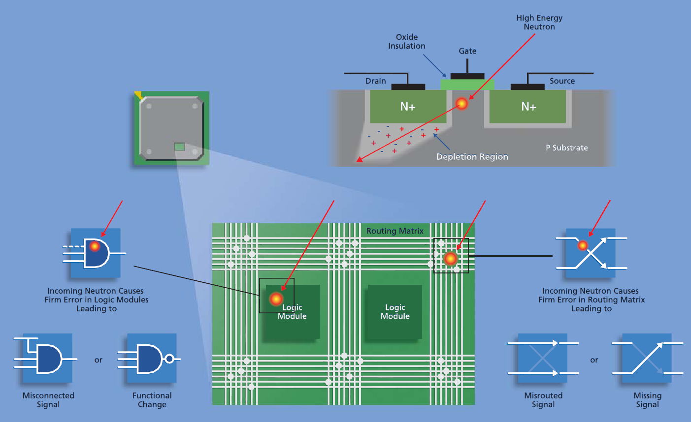
Figure ‑ Effects of Newton’s on SRAM FPGAs (30)
Another form of radiation which poses risk to FPGAs is alpha radiation. Brogley (3) raises concerns of alpha particles emitted from plastic moulding compounds which are used in semiconducting packaging. This is because the semiconducting die is within close proximity of the packaging. These alpha radiation particles are emitted by naturally occurring radioactive isotopes which are generated by impurities, primarily uranium and thorium in IC package moulding compounds. This is still an issue today despite the low alpha compounds used in the manufacturing process (3) (30) (31).
As FPGA fabrication advances for SRAM based FPGAs, there is a greater gate density for a given real-estate. By shrinking the transistor size, the charge required to switch the transistors also reduces. This increases the risk of the transistors being susceptible to radiation induced errors (27) (32). An example is Thelwell (4) who reports that SEEs for 64 to 256 Mbit devices range from approximately 6E-11 to 6E-16 upset/bit-hr at aircraft altitudes of 40,000ft.
FPGA Fault Detection and Recovery
Avionic systems susceptible to SEU failure will need to detect if a SEU condition has occurred. This prevents invalid data from being propagated through a system or stored in memory. Failure to detect corrupt data could result in a system failure. The preventative action is known to the industry as error detection.
Once the system has detected the error, it needs to be corrected to prevent an accumulation of errors. This can be achieved either by discarding the invalid data and replacing with valid data, which is known as error correction. Alternatively, the system could determine the correct data, which is known as Error Detection and correction. There are numerous published research papers which have discussed error detection and correction techniques for FPGA’s (26) (33). However, many of these methods require off-line testing which prevents the FPGA from processing (27). This is undesirable in critical avionic systems and therefore an on-line testing approach is required. On-line testing would allow the system to remain operating whilst the fault is being corrected.
A fault tolerant system requires four stages
- Detection of the error. To detect a SEU fault condition.
- Confinement of the error. To prevent the error from being propagated through the system causing further errors.
- Recovery of the error. Correct the error either by removal, or by error correction.
- Recovery of the system. Continuation of the system throughout this process without downtime.
Aircraft systems generally have Built-In Test (BIT) which allows the detection of faults, including SEE. However, BIT is only an effective mitigation strategy providing a large percentage of the system and critical components are checked. Also the BIT system needs to be relatively small compared to the overall system being checked otherwise Bargh (12) suggests a recursive scenario where a BIT may be required for the BIT system.
Dual Mode Redundancy
Dual Mode Redundancy (DMR) is available in a couple of variations, such as
- Hot spare. The spare module shadows the master module and takes control should the master fail.
- Double Resource with Reversion. Both master and slave modules are utilised simultaneously, yielding in improved throughput. A failure in one module will result in the system using reversionary mode. This mode has reduced throughput.
- Lockstep. This is where a redundant computer system executes its operations in parallel. The lockstep output can be used to determine if a fault has occurred.
DMR relies on Built-In Test (BIT) or data checking methods and cannot use a voting system. Therefore, DMR can only be used on avionics systems which are not critical, or if there is a backup system available (12).
Triple Modular Redundancy
Triple Modular Redundancy (TMR) is a fault tolerant design where three systems simultaneously perform the same task. Their outputs are compared by a voting system which produces a single output. The voting system can mask out a failed output preventing data corruption from propagating through the system.
When designing a complex system, some of the processes may not be critical, thus it may not necessitate TMR which is expensive, costing about 3.2 times the resource and a twofold increase in timing delays for a full TMR at a logic level (12).
Figure ‑ Detection Mitigation correction system (16)
An alternative option is to use selective TMR; whereby none critical parts of the design may only require duplex or single processors (34). Selective TMR would reduce the overhead and cost without significantly sacrificing reliability. However, this is an engineering decision. For highly critical applications where there is a risk of loss of human life or expensive machinery, Rennels (34) reports that it is likely that massive voting redundancy will always be used. This is based on the assumption that the modules will fail randomly and independently. Whilst this is plausible Rennels does not suggest using different designs for each module. This would reduce the probability that all the modules could fail simultaneously due to an inherent design flaw, and therefore improve the reliability of the system. It should be noted that TMR masks the individual error and cannot determine the cause of the error or correct the error. TMR simply ignores the outputs from the suspect FPGA (35).
Another disadvantage with TMR is that the voting system will introduce a delay into the signal. A paper by YANMEI (16) suggests a solution for systems containing a mixture of critical and none critical timing signals. For mission critical outputs where the signal cannot be delayed even for a short period, a majority voter would be suitable. A 3 state voter is suitable for none critical signals and this is shown in Figure 3‑4.
A three state voter is fed with the FPGAs outputs, and a control signal allows the 3 state voter output to go into a high impedance state. This prevents the corrupted data from propagating through the system. The advantage of a 3 state voter is the lower hardware overhead as this feature is inbuilt into FPGAs. A majority voter is the output voter which reflects the state of the majority of FPGAs outputs. In order for TMR to be most effective, each module should be designed and developed by different companies. This will reduce the probability of a design flaw being inherited in all three modules simultaneously, resulting in a system failure.
Interestingly, Yui (36) performed five tests with low upset rates. When TMR was used, there was a 25% reduction in functional errors observed. When partial reconfiguration was used, functional errors reduced by 40%. When both TMR and partial reconfiguration mitigations was combined there was no functional errors observed, as shown in Figure 3‑5. What this author has shown is that there may not be a single solution to SEU failure, and that we should consider a couple of mitigation techniques for the biologically inspired design.
![]()
Figure ‑ A comparison of frequency of errors to total runs for four possible [21]
The author Yui stressed that “it is however important that scrubbing was enabled, it was important to make certain the upset rate was less than the scrub rate. Overwhelming the test system with more upsets than it is designed to mitigate would produce misleading and erroneous data”
Partial Reconfiguration
Partial reconfiguration provides the ability to reprogram a portion of the FPGA whilst the rest of the FPGA continues to run without interruption (27). The system engineer will need to define which areas of the FPGA during the design phase that will be utilised for partial reconfiguration (35). In addition, the rate of scrubbing needs to be considered to prevent an accumulation of bit errors. A more detailed explanation of the type of scrubbing details can be found in Appendix D.4.4 to D.4.6.
Yui (36) reports that as the density of FPGAs increase, partial configuration will become more important for designers. This allows subsections of a FPGA to be reprogrammed whilst other resources within the FPGA are still running. The results taken from Yui (36) show when TMR is implemented into a design there was a 25% decrease in functional errors. When partial reconfiguration is implemented, functional errors decrease by 40%. When both TMR and partial reconfiguration are used in combination to repair configuration memory upsets as well as user logic upsets, there were no observed functional errors. Therefore, this report indicates that using either technique produces a marginal advantage to the design, however when both are used together the design was found to be immune to SEUs induced functional errors. In order to validate these results, further the experimentation would need to be repeated on a wider range of FPGAs. This would include those with higher density as our research shows these are more at risk to SEU.
Ryan Kenny (37) reports that partial reconfiguration can be beneficial to aerospace applications affected by SEU. However, Heiner (38) states that in order to take advantage of partial reconfiguration, the technique would need to be combined with data configuration scrubbing. However, as discussed previously, there is a conflict when using partial configuration and memory scrubbing techniques together. Therefore, this should be taken into consideration during the design phase.
Radiation Hardening
Radiation hardened FPGAs are based on commercial devices, with a variation to the manufacturing process and architecture. An example is using Silicon on Insulator (SoI) or Silicon on Sapphire (SoS), which is an insulating substrate in appose to a semiconductor. By changing the substrate of the FPGA it can be made less susceptible to ionised radiation. Whilst radiation hardening reduces its susceptibility to SEU, there are some disadvantages such as the relatively low demand compared to commercial devices. Therefore, the cost of radiation hardened FPGA can be prohibitively expensive and they often have significantly lower performance compared to Commercial-Off-The-Shelf (COTS) components (35) (29). Radiation hardened FPGA are antifuses or flash based, which results in reconfiguration limitations and generally smaller capacities compared commercial parts.
An Actel RH1020 radiation hardened FPGA was selected to determine its susceptibility to ionised radiation. An extract from the datasheet is shown in Figure 3‑6. This specifies a maximum total dose of 300K rad (Si). There is immunity to latch-up and less than 1×10⁻⁶ errors/bit-day.
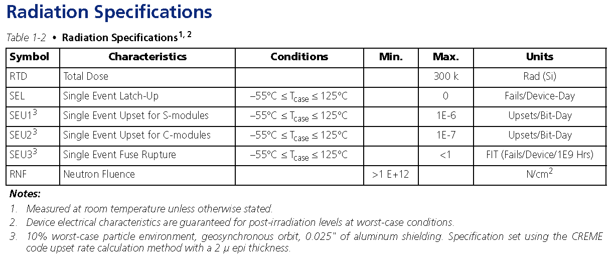
Figure ‑ Actel Radiation Specification datasheet extraction (39)
A radiation report by Xilinx states that very few hard faults were detected during test, and that almost all faults were SEUs in the SRAM. No permanent faults were detected, and reconfiguration of the device was sufficient to regain full functionality after the occurrence of a SEU (16). Had the author Yanmei been more precise in his book to detail the tests more thoroughly, e.g. given details stating the radiation doses used, it would therefore be easier to make a more accurate comparison to the other experiments.
System Reliability
Since the reliability and safety of the avionics system can be affected by SEU, the safety standards needs to be considered. It might be the case that the system safety has already been assessed and based on its critical nature, without the effect of SEU, that triplex redundancy is required. However, if the reliability of the SRAM based FPGA is not within the Mean Time Between Failures (MTBF) then additional mitigation techniques will be required to lower the MTBF (40). In an ideal situation a system failure will result in a repair mechanism to restore the system to a functional state within a specific duration. The probability that a can perform a repair within a desired time is known as the maintainability of the system.
Maintainability M(t) is given by
Equation
Therefore, a relationship between maintainability M(t) and the repair rate µ
Similarly the Mean Time To Repair (MTTR) is given by the
MTTR=
Equation
The availability of a system is the probability that the system is function at any time, and is therefore defined as
Equation
Which can be rationalised to
where
Equation
Therefore, by reducing the MTTR the availability will be increased.
In order to restore system failure back to operation a repair is required. The probability that a system failure will be restored within x time is known as the maintainability of the system. The failure rate is defined as the number of failures per unit time as a fraction of the total population. This is normally expressed as a percentage failure rate per hour / per 1000 hours, or per year. There is a relationship between the maintainability and repair rate and the mean time to repair (MTTR). (20) (31)
Equation MTTR and relationship
MTTR and are related to maintainability M(t) by Equation 9 where t is the permissible time constraint for the maintenance action.
Equation Maintainability equation
For example a failure rate of 5% per 1000 hours and 10,000 components we have average of
The reciprocal of this tells us that the MTBF is
System Availability
The availability of a system is the probability that the system is functional according to expectations at any time during its scheduled working life.
Equation System Availability
This can be simplified down to Equation 11 since
In conclusion, a system with a reduced MTTR will allow for its availability to be increased and therefore a more reliable and economical system.
Discussion
This section has reviewed a number of mitigation techniques and there is evidence to suggest that combining multiple mitigation techniques such as TMR and scrubbing results in a system which is almost immune to SEU failure.
This section is concluded by recommending several design techniques to reduce the risk of SEU failure:
- Minimise the use of RAM and registers, due to their volatility with SEUs
- Combine more than one mitigation technique to improve SEU immunity
- Use radiation hardened components, budget permitting
- Finite state machined should be designed to not have redundant latch-up states which could be entered by an SEU
- Use “One Hot” or Gray code counters in appose to binary counters. This allows SEU’s to be detected by parity checks
This section has explored several mitigation techniques that could be used to improve the tolerability of flight equipment and therefore completes objective 2 of this report
Biological Cells
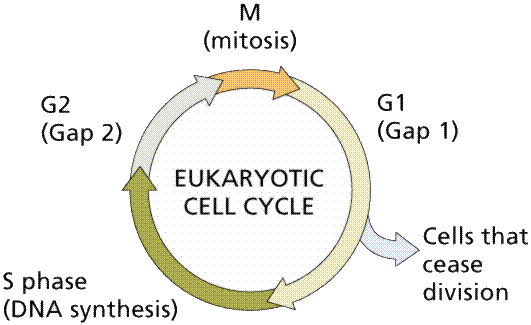
One of the aims for this report is to research how biological cells function and in particular how they can reproduce, reconfigure, and repair.
We shall first review prokaryotic and eukaryotic biological cells to understand their structure and functionality. This should provide some foundation biological knowledge to the reader. We shall then ask relevant scientific questions about how nature allows cells to self-repair and how this can be transcribed into a VHDL behavioural model.
Introduction to Biological Cells
The defence system in vertebrates has evolved over millions of years to what we call the immune system. The immune system has a layered protection system which identifies and kills bacteria and viruses. If a biological defence layer is penetrated then another layer will protect with more complex and ingenious barriers (26).
The human body consists of approximately 60 trillion cells (41), and each of these cells has a specific purpose within the body. The cell is the smallest unit of living matter that can exist on its own and is often referred to as the building blocks of life (42) (43). As part of human development and growth these cells multiple and divide forming.
 Each of the 60 trillion cells contains a genome which is essentially a ribbon of 2 billion characters that is decoded to produce the proteins needed for the survival of the organism. This genome contains the genetic inheritance of the individual and the instructions for both the construction and the operation of the organism. The instructions of the 60 trillion genomes are performed simultaneously during the cells life span (44).
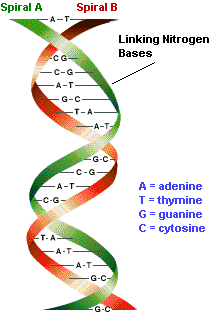
The structure of Deoxyriboucleic Acid (DNA) is that of a long double stranded helix which consists of four repeating nucleotide bases Adenine (A), Cytosine (C), Guanine (G), Thymine (T). An analogy is that the chromosomes can be considered as letters. The letters in a particular sequence form words which are read on a page (45). It is the sequence of these nucleotides which creates the chromosome which results in the human genome cell.
The Meaning of Cells
It was the work of Robert Hooke in 1665 that used the word “cell” in his publication to describe the basic units of cork when viewed under a compound microscope. The biological word “cell” originates from the Latin word Cellula which means small room and is the smallest living entity in order to sustain life (46). The cell can be categorised as either a Prokaryotic or Eukaryotic.
All cells whether Prokaryotic or Eukaryotic have similar division progress (47)
- Replication of the DNA
- Segregation of the original and the replica
- Cytokinesis to end the cells division process
Fundamentally all cells in the human body are all identical and all contain the exact same DNA such as the lung cells execute a different segment of DNA then the skin (42). The exceptions are unfertilized eggs, and sperms which uses a different type of mitosis and only have one set of chromosomes, whereas the other cells in the body has two sets of chromosomes.
Next we shall discuss the difference between prokaryotic and Eukaryotic cells.
Prokaryote cells
Prokaryotes are a group of organisms. They are a self-contained living cell with an outer cell membrane which contains a cytoplasm fluid. The cytoplasm consists of fluids such as water, enzymes, amino acids and glucose molecules. Typical examples of prokaryotes cells are bacteria which are about one-hundredth the size of a human cell and invisible to the naked eye. Prokaryotes lack nuclear membrane so the DNA in bacteria cells is not protected. The prokaryote external membrane has long strands called Flagella which propel the cell. Flagella are not present in all bacteria, and the only human cells which have Flagella are sperm cells (46) (42) (48).
The word prokaryote derives from the Greek meaning Pro (Before) Karyon (Nut or kernel) and is illustrated in Figure 4‑2.
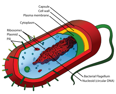
Figure ‑ Prokaryotic Cell Diagram (46)
Eukaryote cells
A Eukaryote is an organism which contains complex structures within membranes. The Eukaryote cells have a nuclear envelope which contains the nucleus and this is the fundamental difference between a Eukaryote and prokaryote.
Eukaryote cells also contain other membranes such as mitochondria, chloroplasts and the Golgi apparatus. The word Eukaryote derives from the Greek meaning Eu (Good) Karyon (Nut or kernel) and is illustrated in Figure 4‑3. A more in-depth discussion of Eukaryote cells can be found in Appendix C.
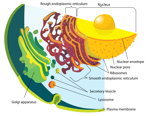
Figure ‑ Endomembrane Diagram (46)
Cell DNA
The DNA contains the genetic information used for the development and functioning of the majority of living organisms. DNA is a nucleic acid and is organised into two long chromosomes. Nucleic acid is a macromolecule comprised of chains of monomeric nucleotides. These molecules carry genetic information of form structures within cells.
The chromosomes are duplicated before the cell divides, known as DNA duplication.
Cellular Repair
DNA is susceptible to mutation by Oxidizing agents, Alkylating agents, Electromagnetic radiation (such as ultra violet and x-rays) and DNA damage. Since DNA Damage and DNA mutation are fundamentally different (46), we shall discuss both to clarify their differences and how nature allows cells to self-repair.
DNA damage is physical abnormalities in the DNA such as single and double strand breaks in the helix. Providing there is redundant information available, such as undamaged DNA sequence in the complementary DNA strand, the enzymes can use a copy of the healthy DNA strand to repair the damaged strand. If the cell’s DNA remains damaged the transcription of the gene can be prevented and the translation into a protein blocked. Also the cellular replication process can also be blocked, as shown in Figure 4‑4 which results in the cells dying.
DNA mutation is where the base sequence of the DNA is changed and if these changes are not corrected the mutated cells could produce fault proteins (Ameno acids). A mutation cannot be recognised once the base change is present in both DNA strands. Therefore, as the cells replicate, so does the mutation.
Mutated cells which do not undergo a process known as programmed cell death (apoptosis) continues to divide are known as cancerous cells. Evolution has responded with two known DNA repair mechanisms which have been categorised as
1) Body enzymes directly repair DNA
2) Damaged region is removed and gap filled by DNA synthesis
Many cells communicate with each other by secreting chemical signals into the extracellular fluid. Some cells secrete regulatory molecules such as hormones and neurotransmitters into the blood stream using a process called trioxide. The chemical signals are targeted for distant cells. These signals perform functions such as growth regulation, development, and organisation. Due to technological limitations, it is currently not possible to implement such techniques into a VHDL behavioural model and is therefore outside the scope of this report. However, it is interesting to understand how nature as responded.
However, what we can learn from that human body is that it is capable of tolerating singular cell damage since the body is not solely dependent on a singular cell. Therefore, by designing the VHDL behavioural model using a cellular approach we can have confidence that the system will continue to operate even with multicellular failure.
Evolvable Hardware
A comparison of the defence system of the human immune system and the hardware protection of a FPGA is shown in Table 4‑1. Bradley (26) considers the atomic barrier and physiological defence mechanism to already exist with current SRAM based FPGAs. Therefore, we shall focus on the innate & acquired immunity mechanisms.
|
Defence mechanism |
Human immune system |
Hardware protection |
|
Atomic barrier (physical) |
Skin, mucous membranes |
Hardware enclosure (physical/EM protection) |
|
Physiological |
Temperature acidity |
Environmental settings (temperature control) |
|
Innate immunity |
Phagocytes |
N-modular redundancy Radiation Hardening Error Detection & Correction |
|
Acquired immunity |
Humoral immunity. Cellular immunity |
? |
Table ‑ Embryonic and hardware layers comparison (26)
The biological definition the innate immunity is one that provides immediate defence against pathogens. This is a defence which knows how to respond to a given situation. For example a TMR system has data corruption on the output, thus it ignores the outputs from the suspect module. Biologically, an acquired immunity is where the immune system has the ability to recognise and remember the pathogens. It is able to generate immunity based on its condition and develop greater defence against pathogens each time it is encountered. This is a significant step, from the innate immunity, and we need to evaluate how we can model this on silicon. The question is how can we recognise and remember SEU’s? Even if we can remember where the SEU’s occurred they are going to impact the silicon in random location and have a temporary effect. This raises the question whether remembering the SEU benefit the design, and it most probably does not. The problem with ionised radiation is that this is an external influence that can only be resolved by changing the material properties used, which is radiation hardening. It is not possible to grow new silicon, or to repair silicon with current technology (42). Therefore, our approach is limited to isolate and bypass the impacted area on the FPGA.
So to hypothesise, our body consists of 60 trillion cells, and damaging a couple of cells does not impact the body. So, the first step is to modulise the FPGAs design into self-contained cells. The FPGA also requires sufficient quantity of spare cells which can be used to replace faulty cells. An important consideration on deciding how the FPGA responds to a defective cell, and this is known as cell replacement.
Discussion
We have discussed the pathology of biological cells and reviewed some of the cellular defense mechanisms formed by nature. The research has demonstrated that the human body can continue to survive despite continuous cells dying or cells damaged/mutated due to
- Massive redundancy of spare biological cells
- Apoptosis (Programmed Cell Death)
- Redundant information (two copies of DNA strand)
It is not possible to grow new cells on the silicon. Therefore, this section concludes that the most appropriate biological defence mechanism that could be adapted into a VHDL behavioural model is n-modular redundancy. This can be achieved by including spare cells in the VHDL behavioural model design.
This section has researched both eukaryote and prokaryote cells with detailed understanding. Therefore, this completes objective 3 of this report
Next, Section 5 of this report shall discuss the embodiment of these defence mechanisms into an Evolvable Hardware approach.
Design Methodology
The development the biologically inspired behavioural model in VHDL is based on biological cells and is known as Embryonics (Embryological Electronics).
This section shall discuss the design methodology of the embryonic architecture which includes the design, synthesis, and implementation of the embryonic cluster.
Based on the research in Section 4, we have defined three defence mechanisms used by nature which could be embodied into an embryonic cell. These are:
- Massive redundancy of spare biological cells
Whilst massive redundancy of embryonic cells is not impossible, it is impractical. This is due to the silicon wafer having limited real estate and the limitations in lithography techniques. Of course, as lithography improves, this will allow more densely populated wafers, and as predicated by Moore’s law, the number of transistors is expected to double every two years. However, Moore’s law cannot continue indefinitely. As discussed in section 3.7 we should combine more than one mitigation technique to improve SEU immunity. Therefore, whilst allocating spare embryonic cells is a reasonable mitigation solution it should not be the only defence mechanism used.
In addition, unlike the human body, it is not possible to regenerate damaged silicon. Therefore, once all the spare embryonic cells have been used, any degradation will result in the design ultimately failing.
- Apoptosis (Programmed Cell Death)
Apoptosis is the process of Programmed Cell Death. This can be implemented in embryonic cells using a variety of self-test mechanisms available, as discussed in 0.
It is reasonable to suggest, that a cell failing self-test should be disabled. However, if the cell is still partially useable, then the cell could be allowed to perform specific functions which are not compromised by the type of failure. For example, an embryonic cell might not be able to perform a LOGIC AND function. However, if the cell can still produce the correct response for a LOGIC NOT function, then it would be reasonable to suggest the cell is still useable in the design and should be flagged as degraded and brought back online. This shall be discussed in more depth later in this section.
- Redundant information (two copies of Genome)
Finally, designing hardware with redundant information is once again only limited by the finite resources available on the silicon wafer. This technique shall be considered for the design of the embryonic cell by developing a Genome that contains the configuration data of the entire cluster and shall be copied to each cell. Whilst this will increase the amount of memory required on the FPGA, it will allow the biologically inspired design to more closely relate to the Eukaryote Cell.
Several research centres such as University West of England, University of York and Logic Systems Laboratory at the Swiss Federal Institute of Technology, Switzerland have developed Embryotic cells with fault tolerance. The University of York has focused on a POEtic model. This model was reviewed and outside the scope of the report. However for completeness, the reader may find an overview of the POEtic model in Appendix 0.
There was no existing embryonic VHDL behavioural model available in the public domain to build upon for this project. Therefore, the author decided to develop bespoke firmware specifically for this paper.
Before the embryonic cluster was designed, the following criteria was defined.
Embryonic Cell Criteria
- Each embryonic cell shall have the capability to operate as a Logic AND, OR NOT gate
- It shall have the capability to perform the function of a half adder and product the correct logic response to a given input
- The embryonic cells shall have input to simulate a SEU fault condition
- A faulty cell shall be automatically detected and taken offline. The faulty cell shall not be used for the function whilst in a faulty state
- A faulty cell shall be automatically replaced by a spare cell in the cluster
- Each cell shall have internal memory to store the Genome
- Each cell shall have the ability to automatically access, store and retrieve any part of the Genome without any external input
- Each cell shall provide test outputs such as state number, faulty signals to permit cell diagnosis
- The cluster shall have a minimum of 12 cells
Embryonic Cell Constraints
- The design shall use a EP20K200EFC484-2X FPGA
- The behavioural model shall have a maximum of 8320 logic cells. (Limitation of FPGA used in project)
Brainstorming Biological Cells & Embryonic Cells
During the project, a brainstorming exercise was used to evaluate both the biological and eukaryotic cells. This was first used to understand the make-up of the biological cells, and then how this can be modelled in a VHDL behavioural model. The results from this brainstorming are shown in Figure 5‑1 & Figure 5‑2.
Figure ‑ Brainstorming for Biological Cells
Figure ‑ Brainstorming to Eukaryotic Cells
Half Adder
The Half adder shall be reference throughout the remainder of this report, so we’ll quickly review the basic principles of what a half adder does.
Electronic devices such as calculators are capable of performing very complex operations which is built on basic arithmetic, such as the addition of numbers. For example multiplication (4*3=12) is the same as adding multiple copies of the same number together (4+4+4=12).
A half adder adds two 1-bit binary numbers A & B together to produce two outputs S and C which are called Set and Carry respectively.
Whilst the half adder does allow for a carry out (C) it does not have the ability of carry in. If a carry in was required, then a Full adder should be used. The half adder truth table is shown in Table 5‑1. A half adder can be designed using one exclusive Logic OR gate, Logic AND gate as shown in Table 5‑1. The half adder shall be used later in this report to demonstrate the functionality of the embryonic cells operating together.
|
Input |
Output |
||
|
A |
B |
Set (s) |
Carry (C) |
|
0 |
0 |
0 |
0 |
|
0 |
1 |
1 |
0 |
|
1 |
0 |
1 |
0 |
|
1 |
1 |
0 |
1 |
Table ‑ Half Adder Truth Table

Figure ‑ Half Adder Logic Diagram
Real-Time Fault Recovery
A system is defined as being real time if it depends on logical correctness and temporal correctness. Tyrrell (49) states that the first principle of fault recover is that “no fault recovery method can be legitimately proclaim efficacy until it is proven to be both logically and temporally correct.” Tyrrell further explains that:
Logical correctness is when the system performs all its assigned tasks and functions according to specification without failure.
Temporal correctness means the system is guaranteed (repeatedly) to perform these functions within explicit timeframes. However, it is outside the scope of this report to develop an embryotic cluster which addresses the temporal correctness. There are two recommended methods to ensure temporal correctness which are: Redundancy and or Multiplying the clock frequency.
Partial Reconfiguration using Embryonic Cell Redundancy
If a faulty cell in the FPGA is detected, a partial reconfiguration response is trigged. The aim is to allow a system to continue operating without being interrupted. There are three known methods of cell replacement which are Row / Column Elimination, Row & Column Elimination and Cell Elimination, each using a two dimensional array of logic elements
i) Row Elimination / Column Elimination. A failure of one cell causes the elimination of the entire row of interconnecting cells, this is demonstrated below in Figure 5‑4, Figure 5‑5, Figure 5‑6. The row is replaced by the row to the north until a spare cell is reached and the functional array is re-configured. Column Elimination uses similar methodology (42) and is demonstrated in Row-elimination was first proposed by Ortega et al (50) (51).
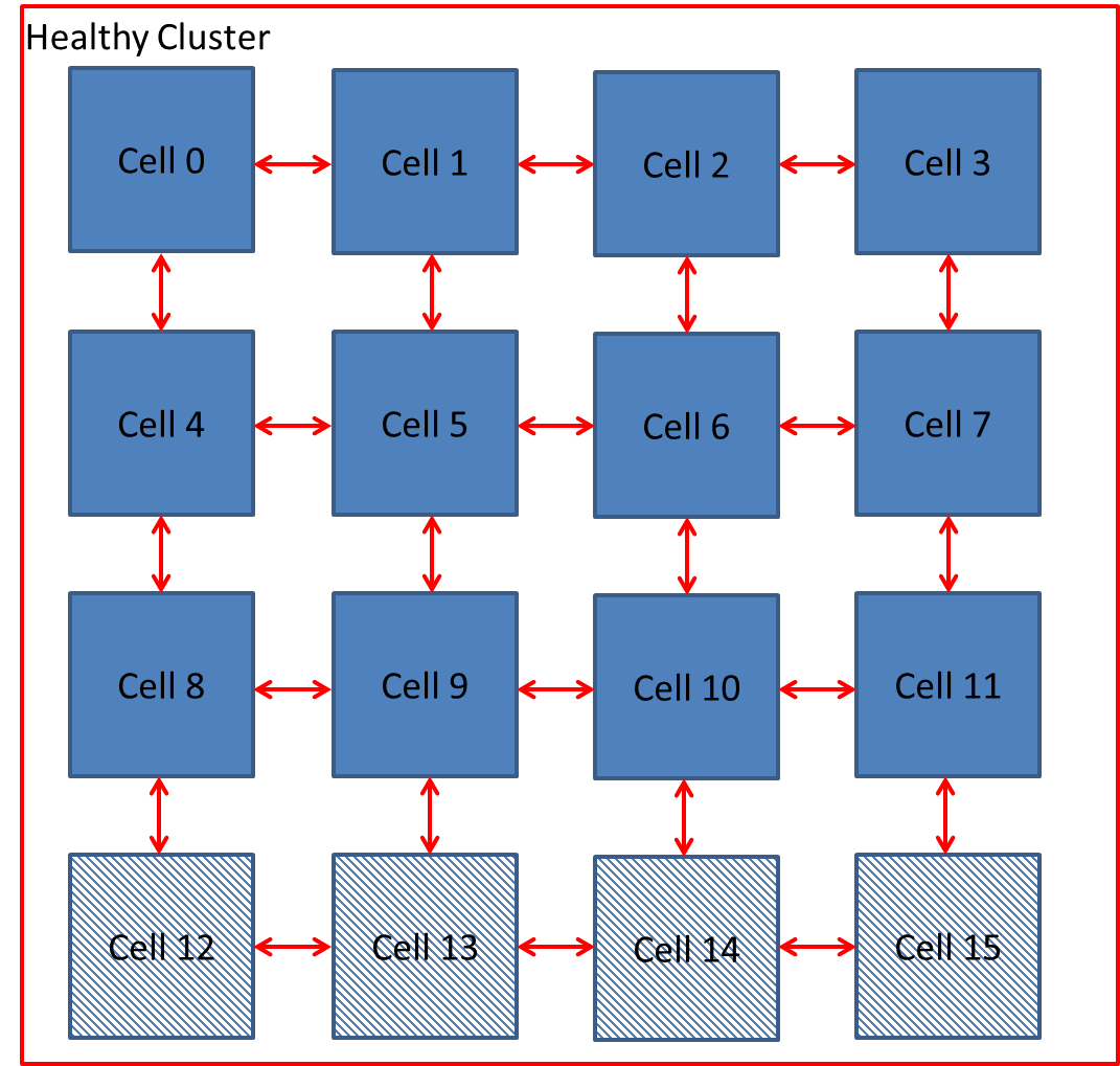
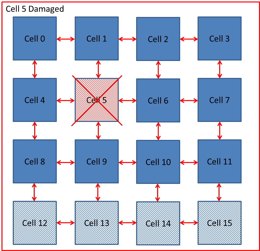
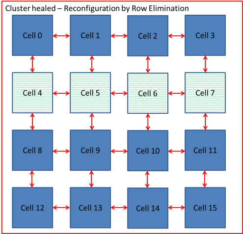
Figure ‑ Reconfiguration by Row Elimination

II) Row and Column Elimination. A failure of a cell will trigger a row or column elimination. However, if the cell does not correctly re-configure then row or column containing the cell will also be eliminated (42). Row and column elimination is used by Canham et al (52) (53).
III) Cell Elimination. Faulty cells are replaced by spare cells to the right of the array. When they are no spare cells available, the row is eliminated. (42). Cell elimination for molecular repair was first proposed by Daniel Mange et al (54) (55).
Xuegong focused on developing an embryotic cell which utilised row and column elimination. A more efficient method would be cell elimination, as only the defective cell would be removed as part of the reconfiguration process. This is demonstrated by a healthy cluster of cells shown in Figure 5‑7 and subsequently cell 5 fails in Figure 5‑8. The repair process works by taking cell 5 offline and replacing with spare cell 12 shown in Figure 5‑9. The reconfiguration process would need to ensure that data is routed to cell 12 automatically without loss of data. Also the cluster would need to perform the reconfiguration process without delaying the output response and therefore have Real-Time Fault Recovery.


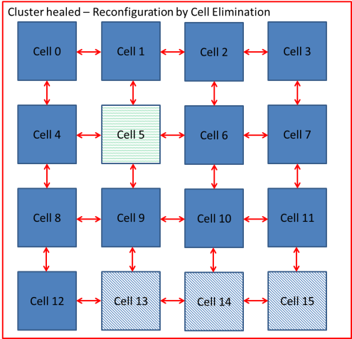
Figure ‑ Reconfiguration by Cell Elimination

Multiply Clock Frequency
The first suggested method of temporal correctness is to operate the internal embryonic cluster at a clock frequency X times higher than the input / output system clock frequency. An example of an embryonic cell operating (hypothetically) 10x higher is shown in Figure 5‑10.

Figure ‑ Example of Embryonic Cell with higher clock freq
Providing the cells internal clock frequency is faster that the external clock frequency, it is feasible that any disruptions could be mitigated by hot-swapping faulty cells for spare cells (cluster reconfiguration) without impacting the temporal correctness. Hence the cluster would produce the output response within the expected time frame.
Cluster Configuration
The biologically inspired design for this project consists of an array of embryonic cells, which shall be referred to as a cluster. Each of the embryonic cells within the cluster is identical in design and can perform any desired Boolean function. This is similar to stem cells in the human body which have the ability to perform any cellular function in the human body. A cluster of 12 cells are illustrated in Figure 5‑11.

Figure ‑ Cluster of 12 embryonic cells
Each embryonic cell contains
- Router. This controls the flow of data to and fro the cell, similar to the Golgi Apparatus (Further information about the Golgi Apparatus can be found in Appendix C.4)
- RAM & RAM Controller. This is the cells memory and defines cells function, similar to DNA
- Control Unit. Controls how all the above mechanisms interact
The author has considered two main cluster configurations to transfer data between embryonic cells which were Method A and Method B, which is discussed next.
Cluster Configuration – Method A
Initially the cluster was going to have the external routers connected in a STAR configuration. This would result in each router being connected to four adjacent cells and up to four adjacent routers. Therefore, a 12-cell cluster would require 6 routers, as shown in Figure 5‑12, and a 32-cell cluster would require 21 routers.
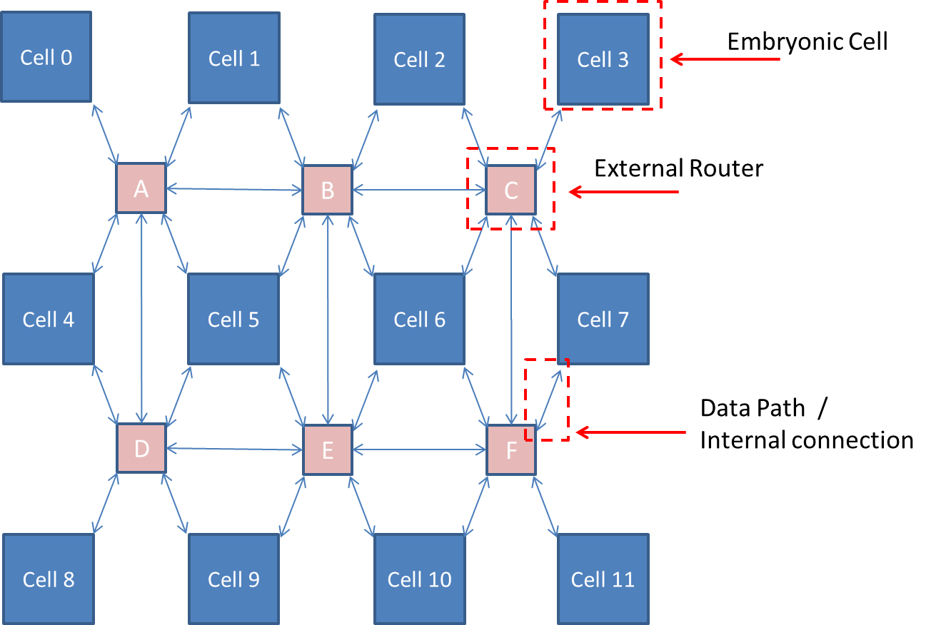
Figure ‑ Cluster Configuration – Method A
A comparison of how many routers is required if the routers are internal or external to the cell, and the results are plotted in Figure 5‑13. This should that less routers are required when they are external to the cell.

Figure ‑ Method A: Number Cells vs Routers Relationship
If a router was damaged, then data would need to be routed through another data path / internal connection. For example, using Figure 5‑12, if we needed to send data from Cell 0 to Cell 9, the data could be routed through routers A->D. or A->B->E. Analysis of the diagram shows that each router could require up to 7 internal connections between cells. A 32-cell cluster would mean each router would require up to 8 internal connections.
Each of these internal connections would be bidirectional. The router would be designated its own IP address and would have the destination IP address. Before the data is sent a packet is transmitted to configure a virtual path. Each router would contain a routing table of connected routers and their status, defining whether they are online or offline. The routing table is broadcasted to other routers in the cluster. Thus each router would know the status of the other routers. If the condition of a router changes or a cell changes status ie enters repair mode, then the routing table is updated and the table is re-broadcasted to the other routers maintaining data freshness.
The routing table could be designed to use the Dijkstra’s algorithm or Link state vector algorithm. A scenario could be that we need to connect cell 1 -> 3. This can be achieved using a route of A->B->C. However, if router B went offline, then an alternative route could be A-> D->E->F->C. A cluster of 12 cells are shown in Figure 5‑14.
Damaged Cell B taken offline
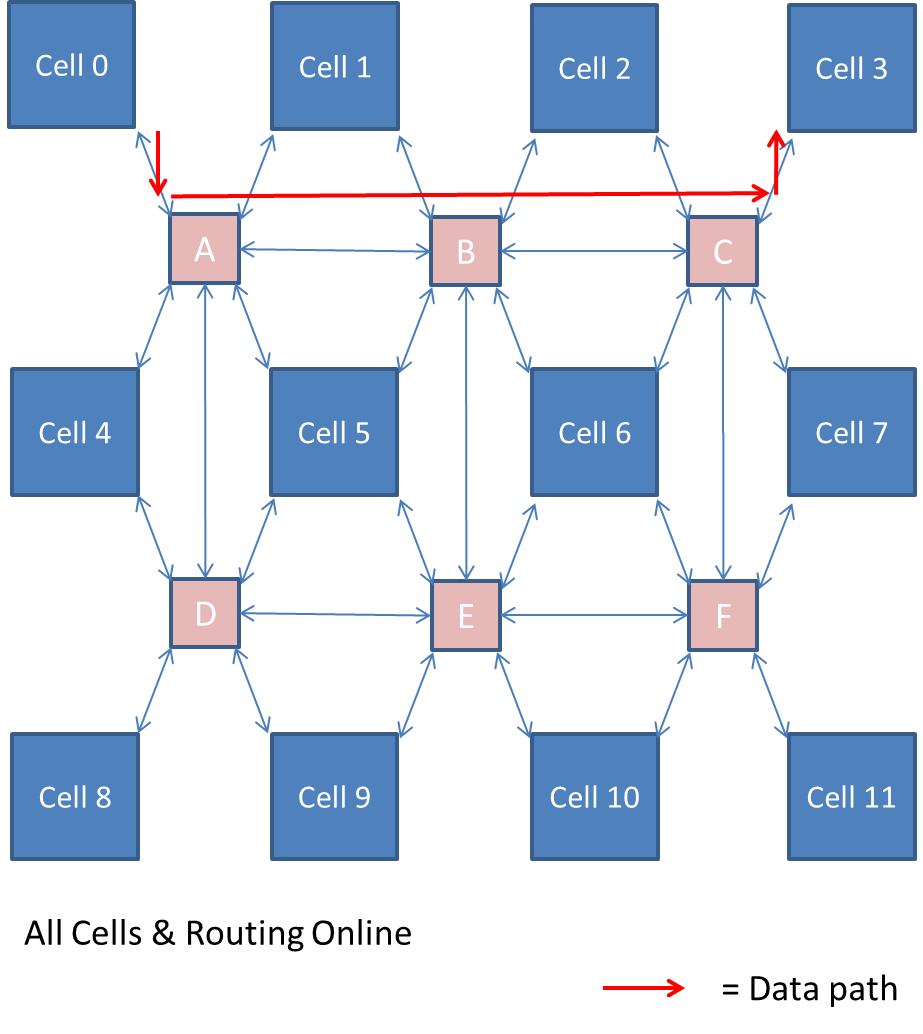

Figure ‑ Illustration of Router B Offline
Routing Table
Each of the cells can be switch online or offline independently. An online cell can process data and product a logic output response. An offline cell will not process data, and its output inhibited.
The routing table, shown in Table 5‑2, was designed to identify which cells are online (Logic 1) and which are off-line (logic 0). The top row shows the Router A to U, which are the 21 routers detailed previously. The table also shows 32 cells in the rows from Cell 0 to Cell 31.
Three different address structures were considered, and they are shown in Table 5‑2. IP address method Alpha uses 6 digits for an X coordinate and 6 digits for a Y coordinate. Each cell increments both X and Y and results in a 12-bit address. This was considered to be an inefficient use of address bits.
Next IP address method Beta was considered. However, this also uses a 12 bit address and was also considered inefficient in term of bits used.
IP Address Method Zeta was then considered which uses Grey Coding. This has the advantage of reducing the address to 6-bits and since the address only changes by 1-bit between adjacent cells there is the potential for error checking.
If the matrix shows an empty field, then Router and Cell are not connected. A Logic 1 in the matrix means the Router and the Cell are connected. For example Router A is connected to Cell 0, 1, 4 & 5.
If Router A went offline due to a failure, then the matrix would be updated such that the Column to Router A was changed from Logic 1 to Logic 0 (Figure 5‑11). If Cell 5 developed a fault, then the Row representing Cell 5 would be updated from Logic 1 to Logic 0 (Figure 5‑12).
This method raises two concerns. Firstly, as the number of cells increase, the number of interconnecting routes between embryonic cells increases exponentially as shown in Figure 5‑15.
Secondly, since the cells and routers are independent there is the potential for either to fail. A router failure could potentially result in a severed connection to healthy cells, and this would cause both router(s) and cell(s) to be taken offline. Therefore, Method B was developed to create a more efficient approach.
Figure ‑ Number of interconnecting signals
|
IP Address method Alpha |
IP Address method Beta |
IP Address Method Zeta (Grey code) |
|
Router |
|
|
|
|
|
|
|
|
|
|
|
|
|
|
|
|
|
|
||||||||||||||||
|
X |
Y |
Whole Address |
Path 1 |
Path 2 |
Path 3 |
Path 4 |
x |
y |
Bin X |
Bin Y |
IP Address |
x |
y |
Grey X |
Grey Y |
IP Address |
Cell |
A |
B |
C |
D |
E |
F |
G |
H |
I |
J |
K |
L |
M |
N |
O |
P |
Q |
R |
S |
T |
U |
|
000000 |
000000 |
000000000000 |
0 |
0 |
000000 |
000000 |
000000000000 |
0 |
0 |
000 |
000 |
000000 |
0 |
1 |
||||||||||||||||||||||||
|
000001 |
000001 |
000001000001 |
AB |
1 |
0 |
000001 |
000000 |
000001000000 |
1 |
0 |
001 |
000 |
001000 |
1 |
1 |
1 |
||||||||||||||||||||||
|
000010 |
000010 |
000010000010 |
BC |
2 |
0 |
000010 |
000000 |
000010000000 |
2 |
0 |
011 |
000 |
011000 |
2 |
1 |
1 |
||||||||||||||||||||||
|
000011 |
000011 |
000011000011 |
3 |
0 |
000011 |
000000 |
000011000000 |
3 |
0 |
010 |
000 |
010000 |
3 |
1 |
||||||||||||||||||||||||
|
000100 |
000100 |
000100000100 |
AD |
0 |
1 |
000000 |
000001 |
000000000001 |
0 |
1 |
000 |
001 |
000001 |
4 |
1 |
1 |
||||||||||||||||||||||
|
000101 |
000101 |
000101000101 |
DE |
AD |
BE |
1 |
1 |
000001 |
000001 |
000001000001 |
1 |
1 |
001 |
001 |
001001 |
5 |
1 |
1 |
1 |
1 |
||||||||||||||||||
|
000110 |
000110 |
000110000110 |
EF |
BE |
CF |
2 |
1 |
000010 |
000001 |
000010000001 |
2 |
1 |
011 |
001 |
011001 |
6 |
1 |
1 |
1 |
1 |
||||||||||||||||||
|
000111 |
000111 |
000111000111 |
CF |
3 |
1 |
000011 |
000001 |
000011000001 |
3 |
1 |
010 |
001 |
010001 |
7 |
1 |
1 |
||||||||||||||||||||||
|
001000 |
001000 |
001000001000 |
DG |
0 |
2 |
000000 |
000010 |
000000000010 |
0 |
2 |
000 |
011 |
000011 |
8 |
1 |
1 |
||||||||||||||||||||||
|
001001 |
001001 |
001001001001 |
GH |
DG |
EH |
1 |
2 |
000001 |
000010 |
000001000010 |
1 |
2 |
001 |
011 |
001011 |
9 |
1 |
1 |
1 |
1 |
||||||||||||||||||
|
001010 |
001010 |
001010001010 |
HI |
EH |
FI |
2 |
2 |
000010 |
000010 |
000010000010 |
2 |
2 |
011 |
011 |
011011 |
10 |
1 |
1 |
1 |
1 |
||||||||||||||||||
|
001011 |
001011 |
001011001011 |
FI |
3 |
2 |
000011 |
000010 |
000011000010 |
3 |
2 |
010 |
011 |
010011 |
11 |
1 |
1 |
||||||||||||||||||||||
|
001100 |
001100 |
001100001100 |
GJ |
0 |
3 |
000000 |
000011 |
000000000011 |
0 |
3 |
000 |
010 |
000010 |
12 |
1 |
1 |
||||||||||||||||||||||
|
001101 |
001101 |
001101001101 |
JK |
GJ |
HK |
1 |
3 |
000001 |
000011 |
000001000011 |
1 |
3 |
001 |
010 |
001010 |
13 |
1 |
1 |
1 |
1 |
||||||||||||||||||
|
001110 |
001110 |
001110001110 |
KL |
HK |
IL |
2 |
3 |
000010 |
000011 |
000010000011 |
2 |
3 |
011 |
010 |
011010 |
14 |
1 |
1 |
1 |
1 |
||||||||||||||||||
|
001111 |
001111 |
001111001111 |
IL |
3 |
3 |
000011 |
000011 |
000011000011 |
3 |
3 |
010 |
010 |
010010 |
15 |
1 |
1 |
||||||||||||||||||||||
|
010000 |
010000 |
010000010000 |
JM |
0 |
4 |
000000 |
000100 |
000000000100 |
0 |
4 |
000 |
110 |
000110 |
16 |
1 |
1 |
||||||||||||||||||||||
|
010001 |
010001 |
010001010001 |
MN |
JM |
KN |
1 |
4 |
000001 |
000100 |
000001000100 |
1 |
4 |
001 |
110 |
001110 |
17 |
1 |
1 |
1 |
1 |
||||||||||||||||||
|
010010 |
010010 |
010010010010 |
NO |
KN |
LO |
2 |
4 |
000010 |
000100 |
000010000100 |
2 |
4 |
011 |
110 |
011110 |
18 |
1 |
1 |
1 |
1 |
||||||||||||||||||
|
010011 |
010011 |
010011010011 |
LO |
3 |
4 |
000011 |
000100 |
000011000100 |
3 |
4 |
010 |
110 |
010110 |
19 |
1 |
1 |
||||||||||||||||||||||
|
010100 |
010100 |
010100010100 |
MP |
0 |
5 |
000000 |
000101 |
000000000101 |
0 |
5 |
000 |
111 |
000111 |
20 |
1 |
1 |
||||||||||||||||||||||
|
010101 |
010101 |
010101010101 |
PQ |
MP |
NQ |
1 |
5 |
000001 |
000101 |
000001000101 |
1 |
5 |
001 |
111 |
001111 |
21 |
1 |
1 |
1 |
1 |
||||||||||||||||||
|
010110 |
010110 |
010110010110 |
QR |
NQ |
OR |
2 |
5 |
000010 |
000101 |
000010000101 |
2 |
5 |
011 |
111 |
011111 |
22 |
1 |
1 |
1 |
1 |
||||||||||||||||||
|
010111 |
010111 |
010111010111 |
OR |
3 |
5 |
000011 |
000101 |
000011000101 |
3 |
5 |
010 |
111 |
010111 |
23 |
1 |
1 |
||||||||||||||||||||||
|
011000 |
011000 |
011000011000 |
PS |
0 |
6 |
000000 |
000110 |
000000000110 |
0 |
6 |
000 |
101 |
000101 |
24 |
1 |
1 |
||||||||||||||||||||||
|
011001 |
011001 |
011001011001 |
ST |
PS |
QT |
1 |
6 |
000001 |
000110 |
000001000110 |
1 |
6 |
001 |
101 |
001101 |
25 |
1 |
1 |
1 |
1 |
||||||||||||||||||
|
011010 |
011010 |
011010011010 |
TU |
QT |
RU |
2 |
6 |
000010 |
000110 |
000010000110 |
2 |
6 |
011 |
101 |
011101 |
26 |
1 |
1 |
1 |
1 |
||||||||||||||||||
|
011011 |
011011 |
011011011011 |
RU |
3 |
6 |
000011 |
000110 |
000011000110 |
3 |
6 |
010 |
101 |
010101 |
27 |
1 |
1 |
||||||||||||||||||||||
|
011100 |
011100 |
011100011100 |
0 |
7 |
000000 |
000111 |
000000000111 |
0 |
7 |
000 |
100 |
000100 |
28 |
1 |
||||||||||||||||||||||||
|
011101 |
011101 |
011101011101 |
1 |
7 |
000001 |
000111 |
000001000111 |
1 |
7 |
001 |
100 |
001100 |
29 |
1 |
1 |
|||||||||||||||||||||||
|
011110 |
011110 |
011110011110 |
2 |
7 |
000010 |
000111 |
000010000111 |
2 |
7 |
011 |
100 |
011100 |
30 |
1 |
1 |
|||||||||||||||||||||||
|
011111 |
011111 |
011111011111 |
3 |
7 |
000011 |
000111 |
000011000111 |
3 |
7 |
010 |
100 |
010100 |
31 |
1 |
||||||||||||||||||||||||
Cluster Configuration – Method B
An alternative method considered for the embryonic design was for each cell to have an internal router, and to eliminate all external routers. Therefore, a 12 cell cluster would have 12 routers, as shown in Figure 5‑16. Likewise, a 32 cell cluster would require 32 routers.
Whilst this has the disadvantage of increasing the number routers required and therefore the number of logic gates required for the embryonic design, this has the advantage that each cell is self-contained. This also closely replicates the philosophy of the Golgi Apparatus routing macromolecules for cell secretion in the Eukaryotic cell, as discussed in Appendix C.4.
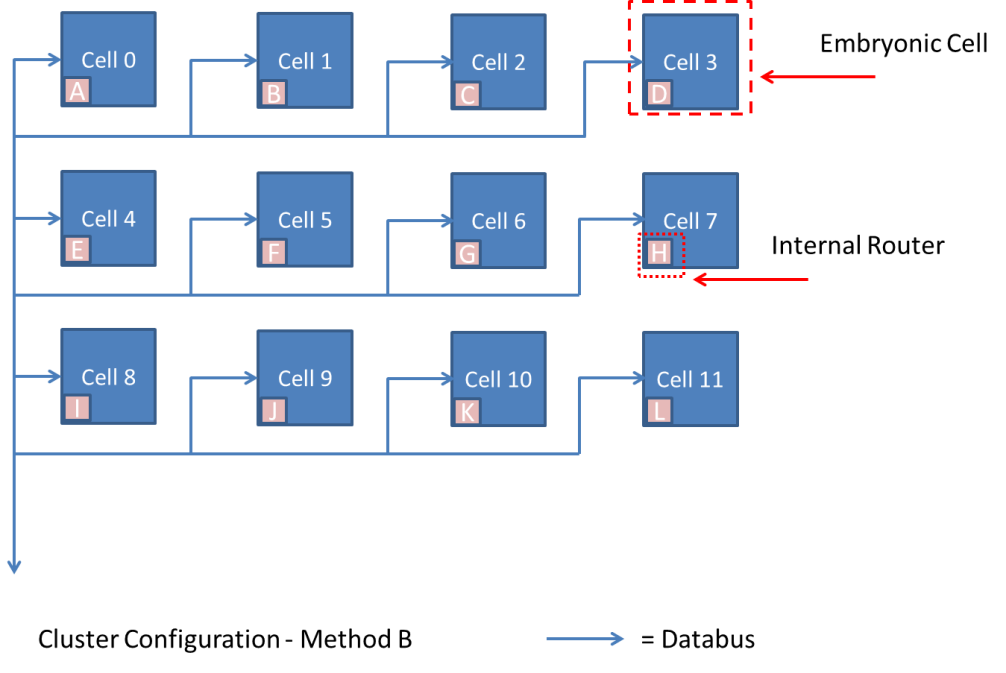
Figure ‑ Cluster Configuration – Method B
Each cell shares access to a 32-bit data bus which reduces the number of interconnections required. However, if two cells try and communicate simultaneously on the data bus the information will be corrupted. Hence, the cells would need to operate to strict protocols which shall be discussed in more depth shortly.
Cell Address
Each cell in the cluster would have three IP addresses assigned. Address A, B & C. The first two address are reserved for the cell input signals, such as the two inputs of a AND gate x & y. The third address is reserved for the cell output, such as the logic output of a AND gate q1. This allows comprehensive control of how data is transferred between cells as shown in Figure 5‑17. Notice that both cells read data from input y and therefore share the same Address 00001.
Each cell would then have the ability to route data to any other cell using a single bus. The number of interconnections is greatly reduced to a single 32 bit bus. To send date to an adjacent cell only a couple of signalling connections and a data connection is required.
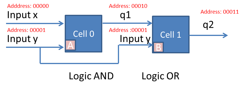
Figure ‑ Example of routing data between two Embryonic Cells
Cell Synchronisation
Another challenge for the embryonic design was to control the flow of data between cells. There are two design issues:
- The cells can be interconnected in any possible combination. A change in the routing will impact the signals transmission time and therefore the temporal correctness of the design.
- Secondly, if a cell is taken offline, the data will need to be automatically re-routed.
Therefore, rather than concentrating on the precise timing, which can vary in a reconfigurable embryonic cell, the author had the idea of using TimeSlots.
The idea was that the TimeSlot would have no predefined duration; they could occur every 1ms, or every 10seconds. In-fact the TimeSlots could vary in duration. What is important about the TimeSlot is that it provides a discrete duration which the cell may process data. This can be considered as polling the cells.
The timing of the TimeSlots shall be independent of the cells clock, and generated by a TimeSlot Generator which will be detailed later in the report. This generator essentially is a circular up-counter.
For example of the TimeSlots being implemented in a half adder is depicted in Figure 5‑18. The half adder consists of 6 combinational logic gates.
 Our first mandatory requirement is that any logic gates directly connected to the Inputs X Y must be in TimeSlot 1.
 Next we can expect the two NOT gates and the top AND gate to produce their output Carry in the subsequent TimeSlot 2.
 Next the OR gate produces the required logic output for TimeSlot 3.
 Finally the required half adder output S is available in TimeSlot 4.


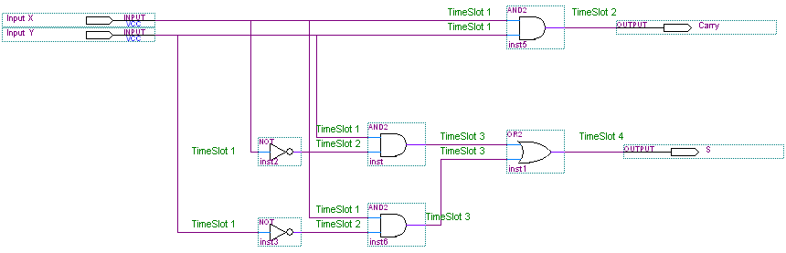
Figure ‑ Half Adder TimeSlot illustration
Therefore, Figure 5‑18 shows that a half Adder will produce all of the required outputs (Carry and S) by TimeSlot 4. Generally the TimeSlot generator will be driven as fast as possible, providing the frequency of the TimeSlot Generator does not exceed the main clock for the VHDL State machines.
Logic Function
The embryonic cells can be configured to perform as a Logic AND, OR, NOT gate.
Therefore, Genome bits 15-16 were allocated in the Genome to define what logic function the cell shall perform once configured, as shown in Table 5‑3. Since only three logic gates was used in this project Logic 11 was not utilised, but this could be utilised as a further project.
|
Logic function |
Genome Bits 15-16 |
|
AND |
00 |
|
OR |
01 |
|
NOT |
10 |
|
Unallocated |
11 |
Table ‑ Logic Function Look-up
Logic Allocation
Providing a cell is not defective it may take responsibility of performing a logic function in the cluster. This single Genome bit defines whether the logic function has been allocated to an Embryonic cell. If the bit is set to 0, which will be the case for all logic functions before confuration, then the logic function is unallocated. The Embryonic cell shall decide whether it has the ability to perform the logic function and set the Allocation bit to Logic 1. Reasons why a cell may decide not to perform a logic function shall be discussed later in the report.
Tag
The tag is allows the Golgi Apparatus to define whether the data is the start, or the end of the Genome. The tag is also used to define whether the data is valid for the Embryonic Cluster. If invalid, then the Golgi Apparatus shall prevent the data from entering a cell. Two bits are allocated for this function, and are defined as shown in Table 5‑4.
|
Bit 31 |
Bit 30 |
|
|
Invalid Tag |
0 |
0 |
|
End of Data |
0 |
1 |
|
Start of Data |
1 |
0 |
|
Invalid Tag |
1 |
1 |
Cluster Configuration Conclusion
A comparison of the number of routers required for each method shows that Method A is more efficient in terms the number of external routers required. Also, Method A can allow multiple data paths to each cell. So even if a router is defective, the data can be re-routed through another datapath without the loss of a cell.
However, the benefits of Method A result in a considerably more complex design to dynamically re-route data.
With method A, it was recognised that in order to implement a 32-bit cell, a significant number of interconnections would be required. For example the each cell should theoretically be able to connect to any other cell which will allow the cluster to be completely reconfigurable. Therefore, an interconnection would be required between every possible combination of cells. Whilst this may be possible for a 9-cell cluster, there would a exponential increase in the number of interconnections required for a 32-cell cluster and therefore it was decided that since Method B shares a bus between cells this would be a better design solution.
Timing of the signals is critical, so engineering intuitively was required to ensure that the signals are guaranteed to be processed between interconnections when required. Method B ensures complete controllability. In addition, the design solution is scalable, and cluster can incorporate a larger array of embryonic cells.
Another advantage of method B is that the Cell is completely self-contained and independent with signal processing. However, this does come with a penalty in that we are using a significant number of additional logic gates to create each Golgi Apparatus which could be avoided using a single unit. This is a design decision, and since we require a robust device method B shall be used.
After significant development of both methods, it was decided to use Method B.
Embryonic Design
This section shall provide a summary of the Genome and an explanation of the primary behavioural modules. A top level block diagram of how the modules interact within the embryonic cell is shown in Figure 5‑19.
The advantage of using the control unit is that it allows the other modules to be completely self-contained.

Figure ‑ Top Level Block Diagram of Embryonic Cell
The reader may find further information including comprehensive schematics and flow charts of the embryonic design in Appendix F & Appendix G.
The Genome
The configuration of the Embryonic Cells shall be controlled by a configuration table called the Genome. This is similar to a Biological Cell configured to function as a lung cell by the DNA.
The Genome is an array of binary words 32-bits wide and each word defines an embryonic cell. Therefore, a cluster of n cells will have a configuration table of n words, as shown in Table 5‑5.
|
Word Bit |
Cell 0 |
Cell 1 |
… |
Cell n |
|
0 |
||||
|
1 |
||||
|
2 |
||||
|
3 |
||||
|
4 |
||||
|
5 |
||||
|
6 |
||||
|
… |
||||
|
… |
||||
|
… |
||||
|
31 |
The configuration table, called the Genome hereafter, defines the complete configuration of the embryonic cells including the cells function, timing, routing configuration, whether active or a spare cell.
The Genome is all the information that is required for the embryonic cells to operate within the cluster, and a breakdown of the Genome is shown in Table 5‑6.
|
Data Function |
Start Bit |
End Bit |
|
Address A |
0 |
4 |
|
Address B |
5 |
9 |
|
Address C |
10 |
14 |
|
Logic Function |
15 |
16 |
|
Allocation |
17 |
17 |
|
Time Allocation A |
18 |
21 |
|
Time Allocation B |
22 |
25 |
|
Time Allocation C |
26 |
29 |
|
Tag |
30 |
31 |
Table ‑ Genome Configuration Table Breakdown
An example of an empty Genome is shown, for illustration purposes only, in Table 5‑7. A practical demonstration of how to populate the Genome to create a behavioural model of the half adder will be explained later.
|
Embryonic Genome Array |
|||||||||||||||||||||||||||||||||
|
Function |
Genome Bit |
0 |
1 |
2 |
3 |
4 |
5 |
6 |
7 |
8 |
9 |
10 |
11 |
12 |
13 |
14 |
15 |
16 |
17 |
18 |
19 |
20 |
21 |
22 |
23 |
24 |
25 |
26 |
27 |
28 |
29 |
30 |
31 |
|
Tag |
31 |
0 |
0 |
0 |
0 |
0 |
0 |
0 |
0 |
0 |
0 |
0 |
0 |
0 |
0 |
0 |
0 |
0 |
0 |
0 |
0 |
0 |
0 |
0 |
0 |
0 |
0 |
0 |
0 |
0 |
0 |
0 |
0 |
|
Tag |
30 |
0 |
0 |
0 |
0 |
0 |
0 |
0 |
0 |
0 |
0 |
0 |
0 |
0 |
0 |
0 |
0 |
0 |
0 |
0 |
0 |
0 |
0 |
0 |
0 |
0 |
0 |
0 |
0 |
0 |
0 |
0 |
0 |
|
Time Allocation C |
29 |
0 |
0 |
0 |
0 |
0 |
0 |
0 |
0 |
0 |
0 |
0 |
0 |
0 |
0 |
0 |
0 |
0 |
0 |
0 |
0 |
0 |
0 |
0 |
0 |
0 |
0 |
0 |
0 |
0 |
0 |
0 |
0 |
|
Time Allocation C |
28 |
0 |
0 |
0 |
0 |
0 |
0 |
0 |
0 |
0 |
0 |
0 |
0 |
0 |
0 |
0 |
0 |
0 |
0 |
0 |
0 |
0 |
0 |
0 |
0 |
0 |
0 |
0 |
0 |
0 |
0 |
0 |
0 |
|
Time Allocation C |
27 |
0 |
0 |
0 |
0 |
0 |
0 |
0 |
0 |
0 |
0 |
0 |
0 |
0 |
0 |
0 |
0 |
0 |
0 |
0 |
0 |
0 |
0 |
0 |
0 |
0 |
0 |
0 |
0 |
0 |
0 |
0 |
0 |
|
Time Allocation C |
26 |
0 |
0 |
0 |
0 |
0 |
0 |
0 |
0 |
0 |
0 |
0 |
0 |
0 |
0 |
0 |
0 |
0 |
0 |
0 |
0 |
0 |
0 |
0 |
0 |
0 |
0 |
0 |
0 |
0 |
0 |
0 |
0 |
|
Time Allocation B |
25 |
0 |
0 |
0 |
0 |
0 |
0 |
0 |
0 |
0 |
0 |
0 |
0 |
0 |
0 |
0 |
0 |
0 |
0 |
0 |
0 |
0 |
0 |
0 |
0 |
0 |
0 |
0 |
0 |
0 |
0 |
0 |
0 |
|
Time Allocation B |
24 |
0 |
0 |
0 |
0 |
0 |
0 |
0 |
0 |
0 |
0 |
0 |
0 |
0 |
0 |
0 |
0 |
0 |
0 |
0 |
0 |
0 |
0 |
0 |
0 |
0 |
0 |
0 |
0 |
0 |
0 |
0 |
0 |
|
Time Allocation B |
23 |
0 |
0 |
0 |
0 |
0 |
0 |
0 |
0 |
0 |
0 |
0 |
0 |
0 |
0 |
0 |
0 |
0 |
0 |
0 |
0 |
0 |
0 |
0 |
0 |
0 |
0 |
0 |
0 |
0 |
0 |
0 |
0 |
|
Time Allocation B |
22 |
0 |
0 |
0 |
0 |
0 |
0 |
0 |
0 |
0 |
0 |
0 |
0 |
0 |
0 |
0 |
0 |
0 |
0 |
0 |
0 |
0 |
0 |
0 |
0 |
0 |
0 |
0 |
0 |
0 |
0 |
0 |
0 |
|
Time Allocation A |
21 |
0 |
0 |
0 |
0 |
0 |
0 |
0 |
0 |
0 |
0 |
0 |
0 |
0 |
0 |
0 |
0 |
0 |
0 |
0 |
0 |
0 |
0 |
0 |
0 |
0 |
0 |
0 |
0 |
0 |
0 |
0 |
0 |
|
Time Allocation A |
20 |
0 |
0 |
0 |
0 |
0 |
0 |
0 |
0 |
0 |
0 |
0 |
0 |
0 |
0 |
0 |
0 |
0 |
0 |
0 |
0 |
0 |
0 |
0 |
0 |
0 |
0 |
0 |
0 |
0 |
0 |
0 |
0 |
|
Time Allocation A |
19 |
0 |
0 |
0 |
0 |
0 |
0 |
0 |
0 |
0 |
0 |
0 |
0 |
0 |
0 |
0 |
0 |
0 |
0 |
0 |
0 |
0 |
0 |
0 |
0 |
0 |
0 |
0 |
0 |
0 |
0 |
0 |
0 |
|
Time Allocation A |
18 |
0 |
0 |
0 |
0 |
0 |
0 |
0 |
0 |
0 |
0 |
0 |
0 |
0 |
0 |
0 |
0 |
0 |
0 |
0 |
0 |
0 |
0 |
0 |
0 |
0 |
0 |
0 |
0 |
0 |
0 |
0 |
0 |
|
Allocation |
17 |
0 |
0 |
0 |
0 |
0 |
0 |
0 |
0 |
0 |
0 |
0 |
0 |
0 |
0 |
0 |
0 |
0 |
0 |
0 |
0 |
0 |
0 |
0 |
0 |
0 |
0 |
0 |
0 |
0 |
0 |
0 |
0 |
|
Logic Function |
16 |
0 |
0 |
0 |
0 |
0 |
0 |
0 |
0 |
0 |
0 |
0 |
0 |
0 |
0 |
0 |
0 |
0 |
0 |
0 |
0 |
0 |
0 |
0 |
0 |
0 |
0 |
0 |
0 |
0 |
0 |
0 |
0 |
|
Logic Function |
15 |
0 |
0 |
0 |
0 |
0 |
0 |
0 |
0 |
0 |
0 |
0 |
0 |
0 |
0 |
0 |
0 |
0 |
0 |
0 |
0 |
0 |
0 |
0 |
0 |
0 |
0 |
0 |
0 |
0 |
0 |
0 |
0 |
|
Address C |
14 |
0 |
0 |
0 |
0 |
0 |
0 |
0 |
0 |
0 |
0 |
0 |
0 |
0 |
0 |
0 |
0 |
0 |
0 |
0 |
0 |
0 |
0 |
0 |
0 |
0 |
0 |
0 |
0 |
0 |
0 |
0 |
0 |
|
Address C |
13 |
0 |
0 |
0 |
0 |
0 |
0 |
0 |
0 |
0 |
0 |
0 |
0 |
0 |
0 |
0 |
0 |
0 |
0 |
0 |
0 |
0 |
0 |
0 |
0 |
0 |
0 |
0 |
0 |
0 |
0 |
0 |
0 |
|
Address C |
12 |
0 |
0 |
0 |
0 |
0 |
0 |
0 |
0 |
0 |
0 |
0 |
0 |
0 |
0 |
0 |
0 |
0 |
0 |
0 |
0 |
0 |
0 |
0 |
0 |
0 |
0 |
0 |
0 |
0 |
0 |
0 |
0 |
|
Address C |
11 |
0 |
0 |
0 |
0 |
0 |
0 |
0 |
0 |
0 |
0 |
0 |
0 |
0 |
0 |
0 |
0 |
0 |
0 |
0 |
0 |
0 |
0 |
0 |
0 |
0 |
0 |
0 |
0 |
0 |
0 |
0 |
0 |
|
Address C |
10 |
0 |
0 |
0 |
0 |
0 |
0 |
0 |
0 |
0 |
0 |
0 |
0 |
0 |
0 |
0 |
0 |
0 |
0 |
0 |
0 |
0 |
0 |
0 |
0 |
0 |
0 |
0 |
0 |
0 |
0 |
0 |
0 |
|
Address B |
9 |
0 |
0 |
0 |
0 |
0 |
0 |
0 |
0 |
0 |
0 |
0 |
0 |
0 |
0 |
0 |
0 |
0 |
0 |
0 |
0 |
0 |
0 |
0 |
0 |
0 |
0 |
0 |
0 |
0 |
0 |
0 |
0 |
|
Address B |
8 |
0 |
0 |
0 |
0 |
0 |
0 |
0 |
0 |
0 |
0 |
0 |
0 |
0 |
0 |
0 |
0 |
0 |
0 |
0 |
0 |
0 |
0 |
0 |
0 |
0 |
0 |
0 |
0 |
0 |
0 |
0 |
0 |
|
Address B |
7 |
0 |
0 |
0 |
0 |
0 |
0 |
0 |
0 |
0 |
0 |
0 |
0 |
0 |
0 |
0 |
0 |
0 |
0 |
0 |
0 |
0 |
0 |
0 |
0 |
0 |
0 |
0 |
0 |
0 |
0 |
0 |
0 |
|
Address B |
6 |
0 |
0 |
0 |
0 |
0 |
0 |
0 |
0 |
0 |
0 |
0 |
0 |
0 |
0 |
0 |
0 |
0 |
0 |
0 |
0 |
0 |
0 |
0 |
0 |
0 |
0 |
0 |
0 |
0 |
0 |
0 |
0 |
|
Address B |
5 |
0 |
0 |
0 |
0 |
0 |
0 |
0 |
0 |
0 |
0 |
0 |
0 |
0 |
0 |
0 |
0 |
0 |
0 |
0 |
0 |
0 |
0 |
0 |
0 |
0 |
0 |
0 |
0 |
0 |
0 |
0 |
0 |
|
Address A |
4 |
0 |
0 |
0 |
0 |
0 |
0 |
0 |
0 |
0 |
0 |
0 |
0 |
0 |
0 |
0 |
0 |
0 |
0 |
0 |
0 |
0 |
0 |
0 |
0 |
0 |
0 |
0 |
0 |
0 |
0 |
0 |
0 |
|
Address A |
3 |
0 |
0 |
0 |
0 |
0 |
0 |
0 |
0 |
0 |
0 |
0 |
0 |
0 |
0 |
0 |
0 |
0 |
0 |
0 |
0 |
0 |
0 |
0 |
0 |
0 |
0 |
0 |
0 |
0 |
0 |
0 |
0 |
|
Address A |
2 |
0 |
0 |
0 |
0 |
0 |
0 |
0 |
0 |
0 |
0 |
0 |
0 |
0 |
0 |
0 |
0 |
0 |
0 |
0 |
0 |
0 |
0 |
0 |
0 |
0 |
0 |
0 |
0 |
0 |
0 |
0 |
0 |
|
Address A |
1 |
0 |
0 |
0 |
0 |
0 |
0 |
0 |
0 |
0 |
0 |
0 |
0 |
0 |
0 |
0 |
0 |
0 |
0 |
0 |
0 |
0 |
0 |
0 |
0 |
0 |
0 |
0 |
0 |
0 |
0 |
0 |
0 |
|
Address A |
0 |
0 |
0 |
0 |
0 |
0 |
0 |
0 |
0 |
0 |
0 |
0 |
0 |
0 |
0 |
0 |
0 |
0 |
0 |
0 |
0 |
0 |
0 |
0 |
0 |
0 |
0 |
0 |
0 |
0 |
0 |
0 |
0 |
Table ‑ Blank Genome table – Method B
Golgi Apparatus Module
The Golgi apparatus is a state machine written in VHDL, and is situation within the Embryonic Cell. The primary responsibility of the Golgi apparatus is to control the flow data entering and exciting the embryonic cell. This is achieved by reading the incoming Genome and verifying whether the data is valid and expected. This is first achieved by reading Genome Tag bits 30 & 31 as per Table 5‑6. A tag with 01b indicates this is the start of the Genome being transmitted and a tag with 10b indicates this is the end of the Genome being transmitted. A breakdown of all combinations of the Genome Tag bits is shown in Table 5‑8.
|
Genome Bit |
Meaning |
|
|
31 |
30 |
|
|
0 |
0 |
No Function |
|
0 |
1 |
Start of Genome |
|
1 |
0 |
End of Genome |
|
1 |
1 |
No Function |
The Golgi Apparatus is a Mealy state machine so the output is dependent on both the current state and the inputs. States 0 to 5 are used during cluster configuration, and once this is complete, the Golgi will remain in state 6. Table 5‑9 provides a summary of each state.
|
Golgi State |
Summary |
|
State 0 |
Setup output signals |
|
State 1 |
Check for incoming Genome verify valid start tag which is ’10’ |
|
State 2 |
Receive remaining Genome. Wait until the control unit is not busy, then load data |
|
State 3 |
This will FORWARD the Genome is the cell is working (state 8) or if the cell has a fault (state 12) |
|
State 4 |
TX State. Relay data from control unit, through Golgi, onto Golgi in next cell |
|
State 5 |
Genome transmitted. Wait for cluster to be fully configured |
|
State 6 |
Cluster is fully configured |
|
State 7 |
Testing Purposes |
Table ‑ State Machine Summary of Golgi Apparatus
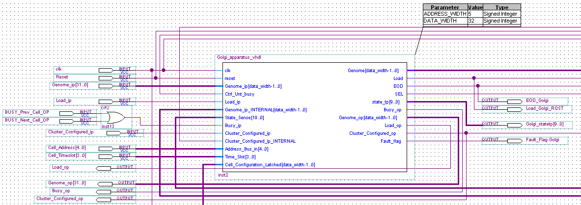
Figure ‑ Golgi Apparatus schematic
Control Unit Module
The Control unit is a mealy state machine with 14 states. This is the most complex VHDL model within this design and it controls all the other state machines within the cell.
The control unit preforms many functions. It ensures the cell starts up in an expected sequence by initialising the cell, performing health tests, clusters configuration, and finally performing the cells function.
The control unit also ensures correct handshaking with each module within the cell, with external cells. This is achieved using busy and AWK flags.
A summary of each state is shown in Table 5‑10.
|
Control Unit State |
Summary |
|
State 0 |
Setup outputs |
|
State 1 |
Initialise the cell. Request an internal Health report and wait for confirmation |
|
State 2 |
BIST in progress, Cell offiline. wait until complete |
|
State 3 |
Read health report from B_Cell. Store in memory |
|
State 4 |
Apoptosis mode. Kill cell. Take cell offline. Forward any Genome onto the next cell. Do not update Genome. Inhibit the output. Prevent any data from being output from MUX |
|
State 5 |
Interface Golgi to RAM. Store the Rx Genome data |
|
State 6 |
Determine if cell can perform required logic function. |
|
State 7 |
This state controls the handshaking with the RAM Controller. We pass the following parameter |
|
State 8 |
Cell is configured. Send Genome onto the next cell |
|
State 9 |
Wait state for rest of cluster to configure |
|
State 10 |
Cluster is configured. Ready to process data. |
|
State 11 |
Setup Logic unit, Process data. |
|
State 12 |
The cell has failed a health test. Forward the Genome onto the next cell. Similar to state 8, but this will trap the cell in this state. |
|
State 13 |
Cell has failed health test, and now waits here unless reset |
Table ‑ State Machine Summary for Control Unit
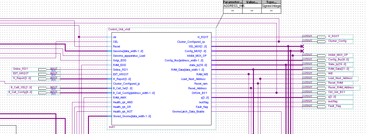
RAM Controller Module
The RAM Controller is the interface between the Control unit and the RAM. It allows access data to be automatically written of read from memory using a mealy state machine.
When data is written to memory, the pointer is automatically moved to the next memory location address. The RAM controller also allows the memory pointer to be automatically reset to the first memory location. The RAM controller outputs an AWK pulse after an instruction has been complete. This allows synchronisation with the control unit.
|
RAM Controller |
Summary |
|
State 0 |
Setup in RAM controller write mode |
|
State 1 |
Setup in RAM controller read mode |
|
State 2 |
Look at next RAM address location. Inform controller we have read end of RAM address |
|
State 3 |
Check that we are not at the end of the RAM Address. Ensures the address counter is only incremented once |
Table ‑ State Machine Summary of RAM Controller
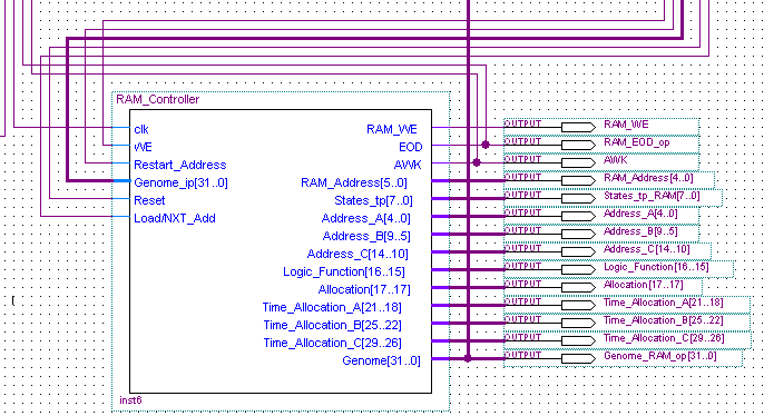
Figure ‑ Ram Controller Block Diagram
Logic Unit Module
The logic unit reads the internally stored Genome bits 15-16 to configure the cell. The configuration allows the cell to perform a specific operation such as AND, OR NOT logic functions.
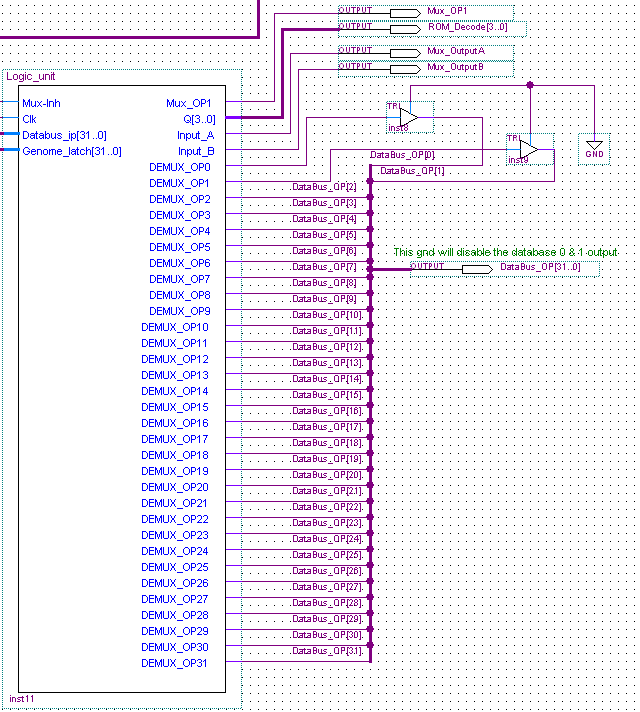
TimeSlot & IPaddress Generator Module
The IPAddress & TimeSlot generators are Moore state machines which have an input clock, enable & reset as shown in Figure 5‑25.
The purpose the TimeSlot generator is to define which cell may have exclusive control over the data bus. The length of time the cell maintains exclusive control of the data bus shall referred to as the TimeSlot Window Duration, see Figure 5‑24. The TimeSlot values are obtained by reading Genome bits 18 to 29.
The purpose of the IPAddress generator is to define which input and output port on the cell has exclusive access of the data bus. The length of time a cells port maintains control shall referred to as the IPAddress Window Duration, see Figure 5‑24. The IPAddress values are obtained by reading Genome bits 0 to 14.
Together, the TimeSlot & IPAddress ensures that every cell and every port on each cell has exclusive control of the bus. This prevents any data collisions which would result in corrupt data and ensures a balanced shared access of the data bus.

Figure ‑ TimeSlot & IPAddress Window Relationship
The IPAddress Generator is driven via an internal clock. Multiplying this clock speed beyond the clock frequency external to the cell could allow real time self-repair as previously discussed in section 5.6.1.
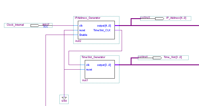
Figure ‑ IPAddress & TimeSlot Generator Schematic
The IP address generator has a 32-bit output bus which is connected to every embryonic cell. The IPAddress generator is a counter which outputs a logic 1 on each address bit at a given time. Once address bit 31 goes high, the counter will restart from 00 h and clocks the TimeSlot generator. The TimeSlot generator has a 5-bit output bus which also connects to every embryonic cell.
Built-In Health Test Module
If the cell detects a fault condition, it should enter a self-diagnostic Built-In Self-Test (BIST) mode. All cell failures would be recorded in the cells internal memory. If the cell detects a fault, this should be stored in the cells memory. A second self-test is performed to verify there are no further defects found.
If the cell does not find the fault during the BIST after 5 attempts it should request support from an adjacent cell. If this still does not find the fault, then it is assumed a glitch of SEU occurred. There is the possibility that if the cell develops a fault, it could prevent the BIST from working correctly. Therefore, the cell could repeatedly perform the BIST, or a faulty cell is brought back online. Repetitive failures could be prevented by limiting a cell to five BIST within a predefined duration. If the number of BIST’s is exceeded, then the cell should request an external health test from an adjacent cell. If the adjacent cell detects an anomaly, this it could have the authority to taken the faulty cell offline.
During development it was considered to use backwards error recovery, whereby the system could return to a previous valid state before the data was corrupted. The advantage is that the system would only need to partially re-perform the algorithm and reduce the number of clock cycles required. This is especially important when considering the real time fault recovery.
All cells would have the ability to perform a health tests and the cells would fall within one of the following four categories:
- Healthy cell. This cell passes all function tests and has the ability to perform any of the functions required from the Genome. The cell is allowed to be taken online during the next reconfiguration process.
- Degraded cell. The cell has been tested and a fault detected. However, the cell is capable of perform at least one of the functions required by the Genome. The cell is marked as being in a degraded state and recorded in the cells internal memory. The cell is then allocated as being a spare and may be switched online during the next reconfiguration process.
- Self-test. The cell is performing a health test to detect any failures. The cell is taken offline and is not permitted to go online during the next configuration process whilst still in the self-test mode.
- Failed cell. The cell has been tested and failed. The cell is unable to perform any of the required functions from the Genome. The cell shall be taken offline and is not permitted to perform any further functions unless stated otherwise.
Subsequent cell failures should also be monitored to prevent a recursive scenario of a cell having poor reliability due to SEU damage. If the cell or the cluster detects that a cell requires a health test due to an anomaly, and this happens three times, then the cell shall be taken offline due to a poor reliability. The disadvantage of this approach is that additional logic is required for the embryotic cells redundancy and additional logic for the majority voter. Finally, there is a risk associated with the majority voting being susceptible to SEU failure.
The development of a Built in Health test was outside the scope of the dissertation and shall not be further developed in this report. However, to permit a SEU failure, test input signals to simulate the function of Built in Health test was used. Future development could remove these simple test signals and replace with a robust Built in Self-test module.

Figure ‑ Input signals in-place of Built in Self-Test module
VHDL Hierarchy
VHDL allows either a bottom up approach using gates or a top down approach by describing the behaviour of the design. This Embryonic cell was designed using VHDL behavioural model in Quartus II.
There are six primary modules to the design.
- Control Unit
- Golgi Apparatus
- RAM Controller
- Logic Unit
- TimeSlot & IPaddress Generator
- Built in Self-Test
The hierarchical approach allowed the embryonic design to be broken down into modules. Each module was developed and tested independently before being implemented into the embryonic cell. This allowed a module to be thoroughly tested before being tested as part of a system level test. The hierarchy of the design is shown in Figure 5‑27.
Module Level
Module Level
Module Level
System Level
Figure ‑ Hierarchy of Embryonic Cluster
The design of the cluster used a modular approach. Each module was tested to ensure the state machined operated as expected with a simulated signal. The modules where then connected together and further debugging performed. An advantage of using a using a modular design is that it is generally accepted that costs are proportional to the square of the number of logic gates in a circuit. Partitioning a circuit into for example four parts reduces the testing problems of each part by a factor of sixteen in comparison to the overall circuit (31).
Once the first embryonic cell was designed and verified to function correctly, it was replicated into two embryonic cells. Further development was required to ensure correct handshaking between the cells once connected. Testing involved injecting a Genome into Cell 0, which was processed and forwarded to Cell 1. Further cells were added to the design 1 at a time and system level tests performed at each stage. This process was repeated until each of the 12-cells could successfully transfer the Genome and self-configured.
Figure ‑ Top Level System Overview
Fault Detection of state machines
Throughout the development of the VHDL, vector fault signals was used to indicate the current state. Also, fault flags were used to indicate if the state machine was in an unexpected condition. Under these circumstances a flag is set high, and the state machine is reset. This was used to validate that the state machines were reacting as predicted by the k-maps. Each of the fault flags are connected to an output pin which is visible from the top level entity. This was used during functional testing on the NIOS demonstration board to verify that none of the state machines was experiencing any unexpected conditions.
For example the following code in the Golgi Apparatus would output a 10-bit vector indicating that the Golgi Apparatus was currently in state 0.
91 — Test signal. Indicates the current state
92 state_tp<=”0000000001″;
Failure Modes and Effects Analysis
The system design has been assessed for potential failure modes. This classifies the severity, likelihood and to establish how detectable the potential fault is. This produced a Risk Priority Number (RPN) which enables the prioritisation of mitigation action. The FMEA steps are shown in Figure 5‑30.
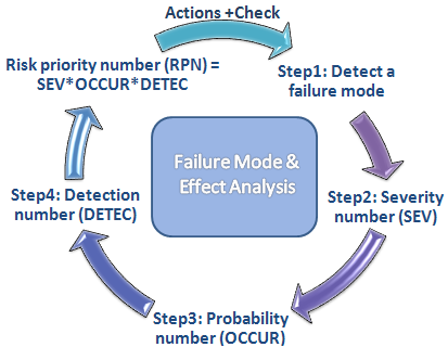
The FMEA in Table 5‑12 shows there is a high risk associated with a track short circuit and nodes not being connected during the design phase. The high rating was because the interconnecting signals are present within each module, and also interconnects each module. As a result, some faults may not be detectable until module level which is more complex to diagnose.
Table ‑ Failure Modes and Effects Analysis
Discussion
This section has reviewed using internal vs external routers, and the technical review has shown that a design using internal routers uses between ~29% to 75% less routers than a design using external routers. However, internal router failure can result in working cells having no data path and being taken offline.
Partial reconfiguration can be performed by row/column/cell replacement. Cell replacement shall be used in the final design because only the defective cell(s) are taken offline, unlike with column/row replacement. It is anticipated that using cell replacement will increase the complexity of the design since data will need to be re-routed during the reconfiguration process. As previously discussed, using multiple mitigation techniques improves the effectiveness against SEU failure. Therefore, we have also reviewed the possibility of increasing the clock frequency to ensure temporal correctness. However, to remain within the project scope, cell replacement will be sufficient to demonstrate fault tolerance.
The FMEA shows the potential failure modes within the system and has highlighted that a high risk associated with a track short circuit and nodes not being connected during the design phase. Controls have been recommended as preventive action.
During this stage, the VHDL behavioural models have been developed using Quartus II. The firmware can be found in Appendix H and on the CDROM included in this report.
This section has discussed how the embryonic cells are going to be developed and the decisions made during this process. Therefore, this successfully completes objective 4 of this report.
Verification Tests
This section shall explain some of the verification tests performed at module level before integrating into the embryonic cell.
Given the complexity of this design, it was decided to demonstrate a selection waveform response during the verification process. Further waveform simulations taken from the verification tests can be found in Appendix E.
Loading Genome into Cluster
Initially, we shall demonstrate that the Genome can be transferred to an embryonic cell and stored within its internal memory. Then the cells transmit the Genome to its neighbouring cell until the cluster is fully configured. At this stage we are only confirming the embryonic cells can process and store a Genome and are not concerned with the details of the Genome since this will be reviewed in Section 7.
The Genome used in this demonstration will configure 6-embryonic cells within the cluster. It can be observed from this waveform that the LOAD_IP signal pulses 6 times, each pulse confirms a cell has received a Genome. In order for the cluster to become configured, the Genome needs to be passed to 6 working embryonic cells as visually represented in Figure 6‑1. When the 6th embryonic cell reads the Genome it automatically identifies that no further embryonic cells are required and thus raises its ClustConfigX flag. T
Cell 1
Cell 2
Cell 3
Cell 4
Cell 5
Cell 6
Genome copied to 6 Cells.
Cluster Configured
Figure ‑ Visual representation of Loading Genome into Cluster
The other 5 embryonic cells detect the raised flags and will subsequently raise their own ClustConfigX flag as acknowledgement.
Once the cluster is configured, it needs to perform the logic function defined by the Genome. In this simple example, we are going to demonstrate an Embryonic Cell function as a LOGIC AND gate which is shown in Figure 6‑2. The inputs of the embryonic cell is toggled, and the waveform confirms the correct output response for a LOGIC AND gate.
Therefore, we’ve confirmed that the embryonic cells can read, processed & store the Genome successfully.
We have confirmed that the embryonic cells have successfully communicated with each other by forwarding the Genome. We have also confirmed that the cluster has automatically detected the required 6 embryonic cells have been allocated and informed each other the cluster is configured.
Finally, we have confirmed that the configured cell can produce the correct response of a AND gate. Further verification tests demonstrating an embryonic cell being configured as a Logic OR, NOT gate can be found in Appendix D.2Error! Reference source not found..
For completeness we shall decode the first Genome word in Figure 6‑4 highlighted in green. The explanation can be found in Table 6‑1.
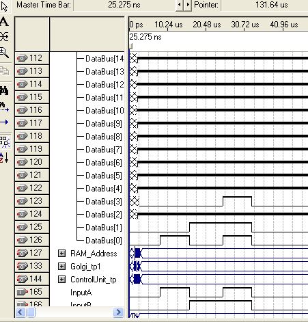
Embryonic Cell Output
Embryonic Cell Inputs
Figure ‑ Cell Verification – Logic AND Function

Green area of Genome to be decoded.
Genome_ip
Genome_op16
Genome_op12
Genome_op8
Genome_op4

Genome_ip
Genome_ip
Genome_ip
Genome_ip
Genome_ip
Genome_ip
Genome_ip
Genome_ip
Genome_ip
Genome_ip
Genome_ip
Genome_ip
Genome_ip
Genome_ip
Genome_ip
Genome_ip
Genome_ip
Genome_ip
Genome_ip
Genome_ip
Genome_ip
Genome_ip
Genome_ip
Genome_ip
Genome_ip
Genome_ip
Genome_ip
Genome_ip
Genome_ip
Genome_ip
Genome_ip
Genome_ip
Genome_ip
Green area is the first Genome word
6 Logic High Loads
Genome Start tag
Genome End tag
Figure ‑ Loading Genome into Cluster
|
Name |
Genome Bit No |
Binary Value |
Comments |
|
Start Bit |
Bit 31 |
1 |
Start Tag. This is the start of the Genome. See Table 5‑6 for reference |
|
Bit 30 |
0 |
||
|
Time Allocation C |
Bit 29 |
0 |
Time Allocation slot 2 assigned to output C |
|
Bit 28 |
0 |
||
|
Bit 27 |
1 |
||
|
Bit 26 |
0 |
||
|
Time Allocation B |
Bit 25 |
0 |
*Time Allocation slot 0 assigned to output B. This means Input A must be directly connected to the source signal since this is the first timeslot |
|
Bit 24 |
0 |
||
|
Bit 23 |
0 |
||
|
Bit 22 |
0 |
||
|
Time Allocation A |
Bit 21 |
0 |
Time Allocation slot 0 assigned to input A. This means Input A must be directly connected to the source signal since this is the first timeslot |
|
Bit 20 |
0 |
||
|
Bit 19 |
0 |
||
|
Bit 18 |
0 |
||
|
Allocation |
Bit 17 |
0 |
This logic function has not yet been allocated to a cell |
|
Logic Function |
Bit 16 |
1 |
The embryonic cell will function as a Logic NOT gate. See Table 5‑6 for reference |
|
Bit 15 |
0 |
||
|
Address C |
Bit 14 |
0 |
The embryonic cells output C is assigned with IP address 210 |
|
Bit 13 |
0 |
||
|
Bit 12 |
0 |
||
|
Bit 11 |
1 |
||
|
Bit 10 |
0 |
||
|
Address B |
Bit 9 |
0 |
*The embryonic cells output B is assigned with IP address 010 |
|
Bit 8 |
0 |
||
|
Bit 7 |
0 |
||
|
Bit 6 |
0 |
||
|
Bit 5 |
0 |
||
|
Address A |
Bit 4 |
0 |
The embryonic cells output A is assigned with IP address 010 |
|
Bit 3 |
0 |
||
|
Bit 2 |
0 |
||
|
Bit 1 |
0 |
||
|
Bit 0 |
0 |
* Since this cell is configured as a Logic NOT gate the secondary output port B is not used.
Table ‑ Breakdown of first 32 Genome Bit for Half Adder
RAM Controller Module
The objective of the RAM Controller is to provide an interface between modules, such as the control unit and the RAM. The RAM Controller provides simplicity such as automatically incrementing the memory pointer on each R/W.
The Control Unit is used frequently to update the contents of the RAM with the Genome and will pass the following parameters for the purpose handshaking.
- sRAM_WE: Do we want to read or write to ram?
- sReset_Address: Do we want to reset RAM Address?
- sReturn_State_Handshaking: Return state when handshaking is complete.
- sLoad_Next_Address: Do you want to load the next RAM address?
Figure 6‑5 shows the control unit in state 7 which sends read and write instructions to the RAM Controller. The signals State_tP(xx) are for test purposes only, which indicate the current state of the control unit. The area shaded in green show initially the MUX output is inhibited. This prevents any change to the cells output. Next the WRITE is enabled which stores the data on the bus in the internal memory. Finally the RAM controller will increment the RAM pointer to the next memory location. The AWK is feedback from the RAM Controller to signal the RAM is busy and that no commands will be processed during this period. This was preventative action against any memory corruption. The waveform validates the Control unit is sending the correct commands to the RAM Controller.
The reader may decode the waveform by using the test point signals and references to the VHDL code in Appendix H.1. However, an explanation is provided below.
The following signals are commands from the Control Unit to the RAM Controller
Reset_RAM. Requests that RAM Address is reset
Load_Next_Address: Requests that RAM points to the next memory location after current command.
Reset_RAM_Address: Requests that RAM resets pointer to the first address location
WE = Logic High sets RAM to write mode. Logic Low set RAM to read mode.
The following signals are confirmation from the RAM Controller
AWK = Logic High confirms the RAM Address has been changed. Used for synchronisation
RAM_EOD_op. Flag to warn the end of the RAM address has been reached.
RAM_WE. Confirms whether the RAM is actually in Read (0) or Write (1) mode
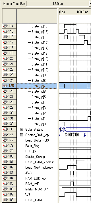
Genome_RAM_op
RAM Controller Commands
Figure ‑ Control unit sending commands to RAM Controller
Finally, a demonstration of the RAM Controlling test signals which breaks down the Genome is shown in Figure 6‑6. 
Figure ‑ Waveform showing RAM Controller Simulation
Genome_RAM_op
TimeSlot & IPAddress Generator Module
This section demonstrates the validation tests for the TimeSlot Generator and the IPAddress Generator.
Both TimeSlot & IPAddress state machines were simulated and verified that the output address ports toggled. The expectation is that initially all of the IPAddress bits will toggle from bit 0 to bit 31. Then cycle back to toggling the first bit. Secondly each time the IPAddress generator reaches the end of its counting sequence it would clock the TimeSlot Generator. An extract of the output waveform of the IPAddress & TimeSlot generator is shown in Figure 6‑7, which verified that both state machines operate correctly.
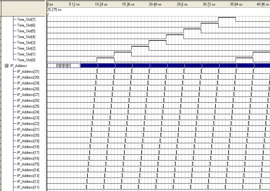
IPAddress generated waveform
TimeSlot generated waveform
Figure ‑ TimeSlot & IPAddress Generator Simulated Waveform
Next, with both modules integrated into the embryonic cells, the expectation is that the cluster of cells initially reads the Genome to configure. Then once the cells are configured and go online, the TimeSlot & IPAddress generators start counting.
As shown in Figure 6‑8 both state machines successfully produced the expected a binary count output once the cluster of cells was configured and switched online. Therefore, both the TimeSlot & IPAddress generators successfully pass the validation tests.
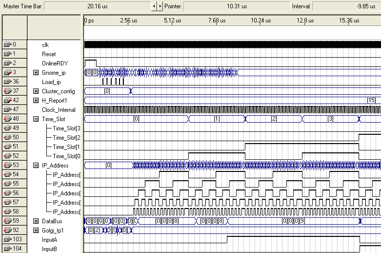
Genome_ip
Timeslot & IP Address Generator starts counting after cluster configured (green and orange area)
Cluster configuring
Cluster of cells configured and switched online
Figure ‑ TimeSlot & IPAddress Generator simulated output waveform
Control Unit & Golgi Apparatus
During development the Control Unit and Golgi Apparatus state machines were tested and validated independently. For clarity this section shall detail the operation of the Control Unit and the Golgi Apparatus state machines together. Due to the scale of the design, it is difficult to show all of the communicate signals. Therefore, a screen of the state test points are shown, which demonstrate the state machine are doing what they are supposed to do.
The reader might wish reference Table 5‑9 for the explanation of the Golgi States and Table 5‑10 for the explanation of the Control Unit state.
Test 1 is the cluster configuration period. The Golgi Apparatus is checking the Genome to ensure it is valid. Providing is valid, its transmitted to the Control unit, and signals the remaining of the Genome can be transmitted. The control unit reads the Genome, and sends the relevant control signals to the RAM Control to store the Genome within the Cells internal memory.
Test 2 The cell is now completed the configuration process. The amended Genome is transmitted to the next embryonic cell, and waits for remaining cells in the cluster to be configured.
Test 3 All the required cells are now configured and online. The cluster can now process data and perform the function of the half adder (assuming a half adder function was required).

Genome_OP19
Test 1 Test 2 Test 3
Figure ‑ Waveform simulation for Control unit & Golgi Apparatus state machines
Simulation Test & Results
This section simulates a cluster of embryonic cells working together to perform a logic function as defined in the objective 5.
It was not anticipated that the design would exceed the number of logic elements available in the FPGA. This only became apparent when all the VHDL modules were combined and replicated for each of the 32 embryonic cells. The initial response was to use an alternative FGPA in Quartus II. However, the higher capacity FPGA’s were not part of the freely available licence. Therefore, the author had three options.
- Redesign to use less logic elements
- Buy a license
- Reduce the number of embryonic cells in the design to reduce the number of logic elements.
It was decided to use the latter since it would not significantly impact the project plan, and it would possible to simulate a half adder in appose to the original full adder which required less logic gates.
Whilst the author decided to configure the cluster as a Half Adder, the reader should be aware this is not a restriction of the design, Infact, the cluster can perform any combinational logic function providing the number of embryonic cells is not exceeded.
Before we review the simulation, we shall briefly review the schematic of a half adder which is shown in Figure 7‑1. This schematic defines how many logic gates are required, which is Two Logic NOT, Three Logic AND, One Logic OR. Since we need 6 combinational logic gates, to configure the cluster to perform as a half adder we need 6 embryonic cells (Remember 1 embryonic cell is required to perform the function of 1 combination logic gate). The schematic also shows the timeslots required for each gate. As a summary, all gates connected to the input signals A & B will always be the first time slot. Then, each gate will allocated the timeslot
This section shall next define the Genome developed for this half adder using the schematic in Figure 7‑1 and the Genome Configuration Table 5‑6. The cluster will first be tested without any faults induced to confirm the cluster can perform the function of a half adder. Then we shall introduce a fault into an embryonic cell using some of the test input signals incorporated during develop to confirm is the cluster can recognise that an embryonic cell is defective and replace with a spare cell.
Half Adder Circuit Diagram

Time Slot 0
Time Slot 0
Half Adder inputs X & Y
Half Adder O/P Sum
Half Adder O/P Carry
Time Slot 2
Time Slot 3
Time Slot2
Time Slot 0
Time Slot 1
Time Slot2
Time Slot2
Time Slot 1
Time Slot 0
Time Slot 1
Time Slot 0
Time Slot 0
Figure ‑ Half Adder Circuit Diagram
Cluster Failure – Root Cause Corrective Action
During the verification tests, two design flaws were detected.
- To test the design, a single cell was configured to perform a function, once the cell passed all tested; a second cell was added to the design. However, as the number of cells increased it was observed that some of the outputs were undefined which results in the cluster not outputting the expected response. Root Cause Corrective Action was undertaken and it was found that the spare cells RAM were undefined. Subsequently, after the cluster was configured, the spare cells were inadvertently taking control of the database and corrupting data. This was subsequently corrected by ensuring the first memory location in RAM was set to a predefined value. A report on how the Root Cause Corrective Action can be found in Appendix Appendix EE.4.1.
- When testing the clusters, cells 13-16 did not produce the expected output response. However, all other cell operated correctly. The fault was caused by two transposed signals on MUX 1 in the logic unit. A detailed investigation which includes the Root Cause Corrective Action can be found in Appendix 0.
Cluster Verification – Half Adder without SEU
The Genome shown in Table 7‑1 was transmitted into the Cluster with no faulty embryonic cells. The aim was to verify the cluster could self-configured as a half adder.
|
Half Adder Genome |
|||||||
|
Not 1 |
Not 2 |
AND 1 |
AND 2 |
AND 3 |
OR 1 |
||
|
Cell 1 |
Cell 2 |
Cell 3 |
Cell 4 |
Cell 5 |
Cell 6 |
||
|
Start |
Bit 31 |
1 |
1 |
1 |
1 |
1 |
0 |
|
Bit 30 |
0 |
0 |
0 |
0 |
0 |
1 |
|
|
Time |
Bit 29 |
0 |
0 |
0 |
0 |
0 |
0 |
|
Bit 28 |
0 |
0 |
0 |
0 |
0 |
1 |
|
|
Bit 27 |
1 |
1 |
1 |
1 |
1 |
0 |
|
|
Bit 26 |
0 |
0 |
0 |
1 |
1 |
0 |
|
|
Time |
Bit 25 |
0 |
0 |
0 |
0 |
0 |
0 |
|
Bit 24 |
0 |
0 |
0 |
0 |
0 |
0 |
|
|
Bit 23 |
0 |
0 |
0 |
0 |
0 |
0 |
|
|
Bit 22 |
0 |
0 |
0 |
0 |
0 |
0 |
|
|
Time |
Bit 21 |
0 |
0 |
0 |
0 |
0 |
0 |
|
Bit 20 |
0 |
0 |
0 |
0 |
0 |
0 |
|
|
Bit 19 |
0 |
0 |
0 |
0 |
0 |
0 |
|
|
Bit 18 |
0 |
0 |
0 |
0 |
0 |
0 |
|
|
Allocation |
Bit 17 |
0 |
0 |
0 |
0 |
0 |
0 |
|
Logic |
Bit 16 |
1 |
1 |
0 |
0 |
0 |
0 |
|
Bit 15 |
0 |
0 |
0 |
0 |
0 |
1 |
|
|
Address C |
Bit 14 |
0 |
0 |
0 |
0 |
0 |
0 |
|
Bit 13 |
0 |
0 |
0 |
0 |
0 |
0 |
|
|
Bit 12 |
0 |
0 |
1 |
1 |
1 |
1 |
|
|
Bit 11 |
1 |
1 |
0 |
0 |
1 |
1 |
|
|
Bit 10 |
0 |
1 |
0 |
1 |
0 |
1 |
|
|
Address B |
Bit 9 |
0 |
0 |
0 |
0 |
0 |
0 |
|
Bit 8 |
0 |
0 |
0 |
0 |
0 |
0 |
|
|
Bit 7 |
0 |
0 |
0 |
0 |
0 |
1 |
|
|
Bit 6 |
0 |
0 |
0 |
0 |
0 |
1 |
|
|
Bit 5 |
0 |
1 |
1 |
1 |
0 |
0 |
|
|
Address A |
Bit 4 |
0 |
0 |
0 |
0 |
0 |
0 |
|
Bit 3 |
0 |
0 |
0 |
0 |
0 |
0 |
|
|
Bit 2 |
0 |
0 |
0 |
0 |
0 |
1 |
|
|
Bit 1 |
0 |
0 |
0 |
1 |
1 |
0 |
|
|
Bit 0 |
0 |
0 |
0 |
0 |
1 |
1 |
|
The X and Y inputs of the cluster was then toggled and the embryonic cells outputs monitored. The expected response of the half adder is shown in the truth Table 7‑2, and the actual waveform response of the cluster is shown in Figure 7‑2.
|
Input |
Output |
||
|
X |
Y |
Carry |
Sum |
|
0 |
0 |
0 |
0 |
|
0 |
1 |
0 |
1 |
|
1 |
0 |
0 |
1 |
|
1 |
1 |
1 |
0 |
Table ‑ Half Adder Truth Table
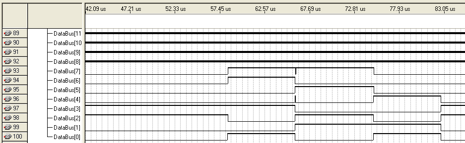
Input X
Input Y
Cell 1 O/P
Cell 2 O/P
Cluster Output C
Cell 5 O/P
Cell 4 O/P
Cluster Output S
Figure ‑ Simulated Waveform of Cluster configured as Half adder. No Faults
The results show that the embryonic cells successfully configured as a half adder and produced the correct output response.
As further confirmation of the cells configuration Figure 7‑3 shows which cells in the cluster are online, and therefore utilised. The waveform signals cluster_ConfigX with a logic 1 represents that the given cell X is online and a logic 0 means the cells is offline. A cell will be offline either because it is a spare cell, or it is faulty.
The simulated results have confirmed the cluster has successfully configured and performed the function of a half adder. This completes objective 5 of this report
Cluster Verification – Half Adder with SEU
Next a simulated SEU fault was injected into embryonic cell 5 and the same Genome was used to configure the cluster. The simulation confirmed that the output of the cluster was exactly the same as Figure 7‑2. This confirms that the cluster can detect & by pass a faulty cell and still produce the valid output response.

Spare cells offline [Logic 0]
Utilised cells online [Logic 1]
Figure ‑ Waveform showing cells online (1) or offline [0]
As further confirmation, Figure 7‑4 shows that the cell 5 has been taken offline due to an internal fault detected and the cluster has utilised a spare cell. This allowed the cluster to still produce the correct response for a half adder.
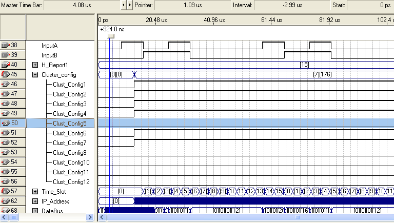
*** Cell faulty – Taken offline ***
Utilised cells online
Utilised cells online
Spare cells offline
Figure ‑ Cluster Configuration bypasses faulty cell
The simulated results have confirmed the cluster correctly detected a faulty embryonic cell, reconfigured to use a spare working cell and still produced the correct output response within the same number of timeslots. This completes objective 6 of this report
Cluster Initialisation Period
The simulation showed that the cell would initialise within 11.76uS. This is the duration required to transmit the Genome into the cluster, all cells to read and self-configure, and the embryonic cells to go online. The waveform simulation is shown in Figure 7‑5.
A finite time is required for the error detection and reconfiguration process. This might not be acceptable for some real time systems. Tyrrell (49) argues that “reconfiguration times are meaningless unless they are put into context”.

Genome_ip
Cells configured and online
Gnome Tx into cluster
Cluster self-configure
Cluster Initialisation Period
Start of Gnome fed into cluster
Figure ‑ Cluster initialisation period
FPGA limitations
During the development of the embryonic cluster it the number of logic elements required exceeded the number of logic elements available to the EP20K200EFC484-2X FPGA (from the development board). Therefore, the simulated cluster of embryonic cells was reduced from 32-cells to 12-Cells.
Several variants of the cluster was developed and compiled to understand how this impacted the number of logic elements required. The compilation was run for 1,4,8,12,16 and 32 cluster of cells and the results are shown in Figure 7‑6.
Figure ‑ Logic Units required per Cluster size
Based on these results, the project was limited to simulating a 12 cell cluster. Therefore, the initial plans of simulating a 2-bit full adder which required 25 embryonic cells (plus spare) was changed to simulating a half adder which only required 6 embryonic cells (plus spare).
Attempts were made to use an alternative FPGA which has more logic units available. This was unsuccessful since the required licence was not available.
Discussion
Originally the cluster was going to operator with 32-embryonic cells. However, the FPGA used in this project did not have sufficient logic element available. Therefore, the behaviour model was simulated with a cluster of 12-embryonic cells. Whilst this is less than the original goal at the start of the dissertation, the principle is the same.
The simulations have shown that the Genome did successfully configure the cluster of embryonic cells to configure as a half adder. This was proven by inputting a binary code, and comparing the output of the cluster to the standard half adder truth table.
Finally, a SEU fault was injected into the cluster. The faulty cell was detected automatically, and the cluster reconfigured to take the faulty cell offline, and allocate a working cell in its place. The results showed that despite the cluster having a faulty cell, the cluster still provided the correct output response, as for the standard half adder truth table.
The design was fully tested and results recorded which can the test results can found in Appendix E.7.
Therefore, this section has successfully completed objectives 5 & 6 of this report.
Conclusions
Introduction
This is the final section of this dissertation which shall first review the original aims and objectives. A summary of what has been learnt by this study shall also be discussed. This section shall also include a review of any achievements and weaknesses found during the research and development phase and a discussion for future research. Finally, this section shall discuss a personal reflection of the dissertation.
Purpose of Study
This dissertation has reviewed the cause and effects of ionised radiation on semiconductor technologies, and how SEU can impact flight safety. The secondary research in this dissertation is quasi-public information which is derived both from internal secondary research within GE Aviation and other aeronautical organisations. The external secondary research is information gathered from 1) Authorities such as the World Health Organisation, 2) Previous studies for single event effects, ionised radiation and embryonic inspired designs. 3) Articles both online and published material 4) Scientific Biological Research
The primary research in this dissertation is derived from the concept of designing and developing a VHDL behavioural model that is inspired from biological cells.
The intent of the embryonic cells was to demonstrate they could
- Perform any logic function, similar to a human cell having the ability to perform the function of any cell in the body by reading a Genome
- To self-configure and perform a logic operation such as an half adder
- Demonstrate fault tolerance, such as a simulated SEU
Summary of Research Outcomes
The secondary research in this dissertation has demonstrated that ionised radiation is a phenomenon which not only exists on the earth’s surface but has also been scientifically proven that radiation levels increases at higher altitudes. The secondary research also showed that SRAM based FPGAs is susceptible to SEU.
Discussion
This report reviewed the innate fault tolerances of biological cells, so they may be used as the foundation for the SEU fault tolerant VHDL behavioural model. The embryonic cells designed in this report used a Genome to store the configuration data, and a copy of the Genome is stored within each embryonic cell. This provides redundancy should the Genome become corrupt. However, this means a higher percentage of the silicon will be allocated to program memory. As the number of embryonic cells increases, so will the required memory space.
Xuegong (42) discussed how the added complexity such as cell elimination requires more transistors and then proposes several solutions includes self-learning in embryonic. An alternative is suggested by Mange (41) who discusses molecular-level technologies such as nanotechnologies, and one of the key issues with nanotechnology is self-replication. So whilst mitigation techniques such as TMR and redundancy are limited by the quantity of silicon available, there may be alternative manufacturing techniques in the future (ie nanotechnology) which may render current solutions obsolete.
There is scope for future development of this embryotic design to reduce the number of logic elements required and therefore produce a more efficient design. Moore’s Law tells us that the number of transistors that can be placed on an IC doubles every two years, whilst this holds true we can expect the density of FPGAs to increase. This means that ionised radiation will pose a greater risk. We can expect continued development into radiation hardened techniques and error detection and correction techniques. We can also expect for critical systems that TMR will remain a preference for many manufactures since this is a tried and tested method.
What the research of biological cells has shown is that none of the embryonic cells should be critical to the functionality of the design. All embryonic cells must be replaceable if the system is to survive a fault and therefore be fault tolerant. By creating an array of common cells which can be configured to perform a particular function is similar to biological cells being defined by the DNA stored within each cell.
The report has attempted to replicate a couple of the biological defence mechanisms. However, biological cells have many layers of defence, and it is probable that there are some biological defence mechanisms that mankind is not yet aware of. So whilst we can improve the fault tolerance of electronics using a bio-inspired approach, the approach will most probably change as we further understand biology. However, we cannot expect silicon will ever have the same fault tolerance as biology since biology and silicon are fundamentally different, and each has their own benefits.
As the embryonic design becomes more sophisticated, the behavioural model architecture will become more complicated. The software/firmware used in aircraft needs to be approved by the flight authorities (FAA or EASA) before it’s certified for flight. If the design is more complicated than required, it will increase the cost, time and scope of the project which in turn affects the deliverables, performance and quality of the product. In addition it will also be more complex to demonstrate that the software is flightworthy. It is the discretion of the customer to decide whether the aircraft equipment is critical to the aircraft, or non-critical such as standby (backup) flight instruments. Avionic equipment which is not critical could use memory scrubbing and the watchdog timer to perform a system reset should a soft error occur. If the system is critical then TMR is more than likely required and will most probably remain the de-facto industrial standard for the foreseeable future. However, just as biology evolved over many years, so will the bio-inspired approaches discussed in this report and could one day become the norm as technology advances.
Achievements & Weaknesses
A considerable amount of time and effort has been dedicated on developing the VHDL. Being able to show the behavioural model does work is a great achievement.
The original goal for this dissertation was to develop a cluster of 32 embryonic cells which could perform the function of a full 2-bit adder. It was not anticipated that the design would exceed the number of logic elements available in the FPGA. The number of logic elements should have been clearly defined in the original constrains. Also, the FPGA’s available on the free license provided should have been added to the risk analysis and constraint to allow better management. This only became apparent when all the functional VHDL modules were combined and replicated for the embryonic cells. The initial response was to use an alternative FGPA in Quartus II. However, the higher capacity FPGA’s were not part of the freely available licence. Therefore, I had three options. Redesign to use less logic elements, buy a license, or reduce the number of embryonic cells in the design to reduce the number of logic elements. I decided to use the latter since it would not significantly impact the project plan, and it would possible to simulate a half adder in appose to the original full adder which required less logic gates. However, as a contingency plan that was not anticipated in the original risk analysis, it was decided to configure the cluster of 12 embryonic cells to perform the function of a half adder. Whilst this is less than the original goal at the start of the dissertation, the principle is the same and it was still possible to demonstrate the operation of the cluster.
When deciding on the objectives, they need to be well defined and measurable. However, when reviewing the project objectives retrospectively they are quite specific which could have resulting in the objectives not being met. For example, objective 2 has been reviewed and re-written. This shows how to convey the objective without applying such as strong constraint on the project. This shall be given more consideration when scoping future projects.
Objective 2 Currently : “Research Eukaryote and Prokaryote cells. Discuss the biological defence mechanisms”
Objective 2 Proposed: “Research two types of biological cells and discuss the biological defence mechanisms”
The majority of research papers reviewed as part of the secondary research favoured Row / Column elimination. This could potentially result in several spare cells required to replace a single defective cell. On that basis, cell elimination was considered to be more efficient, but with more complexity. Deciding to use cell elimination had a risk associated since it required more complexity to re-route data. However, a cell-elimination approach was taken and this was successfully demonstrated in Section 6.
Future research
I recommend that cell replacement is a viable solution and this is something that can be further developed. However, the technical specification of alternative FPGAs should be reviewed to ensure sufficient logic elements are available. This would permit a scalable design (ie 32-cells or higher).
In addition, I recommend including more mitigations techniques which would complement the redundancy method used in this project. For example, multiplying the internal clock frequency would further reduce the risk of temporal correctness.
Finally, the number of signal lines could be reduced by multiplexing. Whilst this could reduce the required logic elements required, this would also result in additional timing complexity.
Personal Reflection
The concept of designing a biologically inspired VHDL behavioural model was a very exciting yet challenging experience.
Project management was important since there was a lot to achieve with both the report and VHDL. I made sure I started the VHDL early in the project. However, I still underestimated how long it would actually take. The only way to keep to the project plan was to increase the number of hours spent on the VHDL. So if this was a real life project, it would most probably be over budget in terms of development.
The project scope was not clearly defined during the early stages, and the scope was developing over time. This scope creep risked not completing the MSc within the agreed timescale. Therefore, I have learnt that I need to spend more time on the project planning before I start working on the solution.
Throughout the dissertation I have maintained a logbook of all my thoughts, idea’s, problems, and solutions. This has been particular useful in maintaining a rhythm of reporting and reminding myself of what I need to do next and what has been discussed during meeting.
The outcome from this dissertation is a success and I feel a sense of achievement and personal satisfaction in achieving my aims. This is down to hard work and listening to the advice of my supervisors for the past year.
Reference List
1. L’Annunziata, Michael F & Prof. Dr.Werner Burkart. Radioactivity Introduction and History. s.l. : Elsevier, 2007.
2. Edwards, R., Dyer, C. and Normand, E. Technical standard for atmospheric radiation single event effects, (SEE) on avionics electronics . s.l. : IEEE Radiation Effects Data Workshop, 2004 . 0-7803-8697-3.
3. Brogley, Mike. FPGA Reliability and the Sunspot Cycle. s.l. : Actel, 2009.
4. Thelwell, L. Single Event Effects Mitigation Strategy. s.l. : GE Aviation, 2008.
5. Sunspot. Wkipedia. [Online] 09 08 2011. http://en.wikipedia.org/wiki/Sunspot.
6. Ionizing radiation. Wikipedia. [Online] 08 07 2011. http://en.wikipedia.org/wiki/Ionizing_radiation.
7. Organisation, World Health. Cosmic Radiation. World Health Organisation. [Online] [Cited: April 20th 2010.] http://www.who.int/ionizing_radiation/env/cosmic/en/index1.html.
8. Administration, Federal Aviation. In-flight Radiation Exposure. s.l. : Federal Aviation Administration, 2006. 120-61A.
9. Copeland, Kyle and al, et. Solar Radiation Alert System. Office of Aerospace Medicine, Washington, DC 20591 : Federal Aviation Administration, 2005. DOT/FAA/AM-05/14.
10. Airways, British. Cosmic radiation . British Airways. [Online] [Cited: April 24th 2010.] http://www.britishairways.com/travel/healthcosmic/public/en_gb.
11. Commission, International Electrotechnical. Process management for avionics – Atmospheric radiation effects – TS 62396-1. 2006.
12. Bargh, R.A. Single Event Mitigation Strategy. Cheltheman : GE Aviation, 2006. SDD16316-1.
13. Normand, Eugene. Single-Event Effects in Avionics. s.l. : IEEE TRANSACTIONS ON NUCLEAR SCIENCE, 1996.
14. —. Single Event Effects in Avionics. Solar Storms. [Online] 16 12 1998. [Cited: 07 09 2010.] www.solarstorms.org/SEUavionics.pdf.
15. Nicole Kerness, Allen Taber. NEUTRON SEU TRENDS TN AVIONICS. s.l. : IEEE Radiation Effects Data Workshop, 1997. 0-7803-4061.
16. LI, YANMEI. A New Approach To Detect-Mitigate-Corct Radiation A New Approach To Detect-Mitigate-Corct Radiation Application. s.l. : IEEE, 2000.
17. RASMUSSEN, ROBERT D. Spacecraft Electronics Design for Radiation Tolerance. s.l. : IEEE, 1988.
18. T. Calinl, M. Nicolaidisl, R. Velazco2. Upset Hardened Memory Design for Submicron CMOS technology. s.l. : IEEE, 1996.
19. Radiation hardening . Wapedia. [Online] 16 7 2010. http://wapedia.mobi/en/Radiation_hardening.
20. Peter Fortescue, et el. Spacecraft Systems Engineering. s.l. : Wiley, 1995. 0-471-95220-6.
21. IEC. Accommodation of Atmospheric Radiation Effects via Single Event Effects within Avionics Electronic Equipment. s.l. : Commission Electrotechnique Internationale. IEC/TS 62396-1 PT1.
22. Ziegler, J F. Trends in Electronic Reliability Effects of Terrestrial Cosmic Rays. United States Naval Academy. [Online] 7 8 2011. http://www.srim.org/SER/SERTrends.htm.
23. LANSCE. LANSCE. [Online] 11 07 2011. http://lansce.lanl.gov/about/linac.shtml.
24. Cyclotron. Wikipedia. [Online] 07 08 2011. http://en.wikipedia.org/wiki/Cyclotron.
25. Ames, Ben. Military & Aerospace Electronics. s.l. : PennWell Corporation, 2004.
26. A Hardware Immune System for Benchmark State Machine Error Detection. Bradley, Daryl. Honolulu, HI : Evolutionary Computation, 2002. CEC ’02. Proceedings of the 2002 Congress on, 2002, Vols. 1. Pages 813 – 818. 0-7803-7282-4.
27. Fay et. al, Dan. Teaching Fault Tolerant FPGA Design for Aerospace Applications. s.l. : IEEE, 2007.
28. Kawai, Hiroyuki. Realization of the sound space environment for the radiation tolerant space craft. s.l. : IEEE, 2006.
29. Hardening FPGA-based systems against SEUs: A new design methodology. Sterpone, L and al, et. NO. 1, s.l. : ACADEMY PUBLISHER, 2006, JOURNAL OF COMPUTERS, Vol. VOL. 1.
30. Actel. Single Event Effects in FPGAs. s.l. : Actel, 2007.
31. Hurst, Stanley L. VLSI Testing. s.l. : The Institution Of Electrical Engineers, 1998. 0-85296-901-5.
32. Anurag Tiwari, Karen A. Tomko. Enhanced Reliability of Finite-State Machines in FPGA Through Efficient Fault Detection and Correction. s.l. : IEEE, 2005.
33. The Bell System Technical Journal. Hammaing, R. W. 2, s.l. : Anerica Telephone and Telegraph Company, 1950, Vol. XX1X.
34. Rennels, David A. Fault Tolerant Computing – Concepts and Examples. s.l. : IEEE, 1984.
35. Jacobs, Adam. Reconfigurable fault tolerance: A framework for environmentally adaptive fault migration in space. s.l. : IEEE, 2009.
36. Yui, C.C. SEU Mitigation Testing of Xilinx. s.l. : IEE.
37. Kenny, J. Ryan and Rupe, David. FPGA Run-Time Reconfiguration: Two Approaches. s.l. : Altera, 2008.
38. Heiner, Jonathan, Sellers, Benjamin and Wirthlin, Michael. FPGA Partial Reconfiguration Via Configuration Scrubbing. s.l. : IEEE, 2009.
39. Actel. Radiation-Hardened FPGAs. s.l. : Actel , 2005.
40. CREME96: A Revision of the Cosmic Ray Effects on Micro-Electronics Code. Tylka, Allan. 6, s.l. : IEEE Transactions on Nuclear Science, 1997, Vol. 44.
41. Mange, Daniel. Biology Meets Electronics: the Path to a Bio-Inspired FPGA. s.l. : Swiss Federal Institute of Technology, 2000.
42. Zhang, Xuegong. Biologically Inspired Highly Reliable Electronic Systems With Self-Healing Cellular Architecture. Bristol : University of the West of England, 2005.
43. Oxford. Oxford Advanced Learner’s Dictionary 7t Edition. s.l. : University Press, 2005. 978-0-19-400116-8.
44. MANGE, Daniel and el., et. EMBRYONICS: A NEW FAMILY OF COARSE-GRAINED FIELD-PROGRAMMABLE GATE ARRAY WITH SELF-REPAIR AND SELF-REPRODUCING PROPERTIES. s.l. : The Swiss Federal Institute of Technology, 1996.
45. Dave. Cellupedia. Cellupedia. [Online] [Cited: 25 08 2010.] http://library.thinkquest.org/C004535/dna_replication.html.
46. Wikipedia. Cell (biology). Wikipedia. [Online] [Cited: 25 08 2010.] http://en.wikipedia.org/wiki/Cell_(biology).
47. Farabee, Michael J. Online Biology Book. Online Biology Book. [Online] [Cited: 25 08 2010.] http://www.emc.maricopa.edu/faculty/farabee/biobk/biobooktoc.html.
48. How Cells Work. How Stuff Works. [Online] 23 07 2011. http://science.howstuffworks.com/environmental/life/cellular-microscopic/cell1.htm.
49. POEtic Tissue: An Integrated Architecture for Bio-Inspired Hardware. Tyrrell, Andy M and el, et. Berlin : From Biology to Hadware: Proc 5th Int Conf on Evolvable Systems: From Biology to Hardware, 2003.
50. MUXTREE Revisited: Embryonics as a Reconfiguration Strategy in Fault-Tolerant Processor Arrays. Ortega-Sanchez, Cesar and Tyrell, Andrew. Lausanne, Switzerland : Proceedings of ICES98, 1998. Vols. Lecture Notes in Computer Science 1478, Springer-Verlag, pp. 206-217.
51. Ortega-Sanchez, Cesar A. Embryonics: A Bio-Inspired Fault-Tolerant Multi-cellular System. The University of York : PhD thesis, 2000.
52. A Hardware Artificial Immue system and Embryonic Array for Fault Tolerant Systems. Canham, Richard O. and Tyrell, Andy M. Genetic Programming and Evolvable Machines, s.l. : Kluwer Academic Publishers, December 2003, Vols. 4 pp 359-382.
53. A Multilayered Immune System for Hardware Fault Tolerance within an Embryonic Array. Canham, Richard O. and Tyrell, Andy M. s.l. : 1st International Conference on Artificial Immune System, 2002. ICARIS2002.
54. The Path to a Bio-Inspired FGPA. Prodan, L, Tempest, Mange, D and Stauffer, A. Edinburgh, Scotland : 3rd International Conference, 2000.
55. Embryonics: A Macroscopic View of the Cellular Architecture. Mange, Daniel, Stauffer, Andre and Tempesti, Gianluca. s.l. : Second International Conference, ICES98, 1998.
56. Education, Nature. Nuclear pore. Scitable by Nature Education. [Online] [Cited: 06 09 2010.] http://www.nature.com/scitable/definition/nuclear-pore-279.
57. Gwen V. Childs, Ph.D. Nuclear Envelope. Cytochemistry. [Online] [Cited: 08 09 2010.] http://www.cytochemistry.net/cell-biology/nuclear_envelope.htm.
58. Test Procedures for the Measurement of Single-Event Effects in Semiconductor Devices from Heavy Ion Irradiation. Arlington. s.l. : Electronic Industries Association, Engineering, 1996, EIA/JEDEC STANDARD.
59. Irom, Farokh and al, et. Investigation of Single-Event Transients in Linear Voltage Regulators. s.l. : IEEE TRANSACTIONS ON NUCLEAR SCIENCE, 2008.
60. Widmer, Tocci. Digital System Principles and Applications. Seventh. New Jersey : Prentice Hall, 1998. 0-13-700510-5.
61. Caffrey, Michael, Carmichael, Carl and Salazar, Anthony. Correcting Single-Event Upsets Through Virtex Partial Configuration. s.l. : Xilinx, 2000.
62. Carmichael et. al, Carl. Correcting Single-Event Upsets with a Self-Hosting Configuration Management Core. s.l. : Xilinx, 2008.
63. G.S.Hollingworth. To Evolve in a Changing Environment. s.l. : IEE Colloquium on Reconfigurable Systems, 1999.
64. Radiation, The United Nations Scientific Committee of the Effects of Atomic. ANNEX E Occupational radiation exposures. s.l. : UNSCEAR, 2000.
65. J.V. Osborn, R.C. Lacoe, D.C. Mayer, and G. Yabiku. Total Dose Hardness of Three Commercial CMOS Microelectronics Foundries. s.l. : The Aerospace Corporation, 1998.
66. Anwar, Md. Tanveer. A novel FPGA Architecture with Built-in Error Correction. s.l. : IEE, 2007.
67. Normand, Eugene. Single Event Upset at Ground Level. s.l. : IEE, 1996.
68. Mohanram, Kartik. Simulation of transients caused by single-event upsets in combinational logic. s.l. : IEEE, 2005.
69. Altera. Cyclone III Device Handbook, Volume 1. s.l. : Altera Corporation, 2010.
70. —. Robust SEU Mitigation With Stratix III FPGAs. s.l. : Altera, 2007.
71. —. AN 539 Test Methodology of Error Detection and Recovery using CRC in Altera FPGA Devices. s.l. : Altera, 2009.
72. TI. TI. Jack Kilby. [Online] [Cited: April 5th 2010.] http://www.ti.com/corp/docs/kilbyctr/jackstclair.shtml.
73. Wikipedia. Integrated circuit. Wikipedia. [Online] [Cited: April 5th 2010.] http://en.wikipedia.org/wiki/Integrated_circuit.
74. Saleh, Abdallah M et al. Reliability of Scrubbing Recovery-Techniques for Memory Systems. s.l. : IEEE, 1990.
75. Fay et. al, Dan. An Adaptive Fault-Tolerant Memory System for FPGA-based Architectures in the Space Environment. s.l. : IEEE, 2007.
76. Miller et. al, Greg. Single-Event Upset Mitigation for Xilinx FPGA Block Memories. s.l. : Xilinx, 2008.
77. IECQ. Why the avionics industry needs IECQ. IECQ. [Online] [Cited: 09 06 2010.] http://www.iecq.org/avionics/need.htm.
78. Barth, J. IEEE NSREC Short Course . NASA. [Online] 1997. [Cited: 06 09 2010.] http://radhome.gsfc.nasa.gov/radhome/papers/slideshow10/SC_NSREC97/sld001.htm.
79. Ionizing radiation. World Health Organization. [Online] [Cited: 10 09 2010.] http://www.who.int/ionizing_radiation/en/.
80. European Aviation Safety Agency. European Aviation Safety Agency. [Online] [Cited: 14 09 2010.] http://www.easa.europa.eu/.
81. Civil Aviation Authority. Civil Aviation Authority. [Online] [Cited: 14 9 2010.] http://www.caa.co.uk/.
82. William, Stallings. Data and Computer Communications. Eigth. NJ : Pearson Education, 2009. 0-13-507139-9.
83. An Architecture for Self Healing Digital Systems. Lala, P.K. and Kumar, B.K. pages 3 – 7 , University of Arkansas : Kluwer Academic Publishers, 2002. 0-7695-1641-6 .
84. Commission, International Electrotechnical. IEC Document: List of Basic Terms, Definitions and Related Mathematics. Geneva, Switzerland, : IEC, 1974. Publication No.271,.
– Project Plan
Project Tasks
This section includes the tasks required to complete the project and also the Gantt chart.
|
Task Name |
Duration |
Start |
Finish |
Predecessors |
|
Preliminary Research |
19 days |
Sun 15/08/10 |
Wed 08/09/10 |
|
|
Review Progress with Assessor |
1 day |
Thu 09/09/10 |
Thu 09/09/10 |
1 |
|
Selection of project |
6 days |
Fri 10/09/10 |
Fri 17/09/10 |
2 |
|
Development of project proposal |
6 days |
Mon 20/09/10 |
Mon 27/09/10 |
3 |
|
Submission of project proposal form |
6 days |
Tue 28/09/10 |
Tue 05/10/10 |
4 |
|
Secondary Research |
21 days |
Wed 06/10/10 |
Wed 03/11/10 |
|
|
Develop understanding of cause of cosmic radiation |
21 days |
Wed 06/10/10 |
Wed 03/11/10 |
5 |
|
Introduction |
11 days |
Thu 04/11/10 |
Thu 18/11/10 |
|
|
Background |
5 days |
Thu 04/11/10 |
Wed 10/11/10 |
7 |
|
Project aims and objectives |
2 days |
Thu 11/11/10 |
Fri 12/11/10 |
9 |
|
Risk Analysis |
2 days |
Mon 15/11/10 |
Tue 16/11/10 |
10 |
|
WBS |
2 days |
Wed 17/11/10 |
Thu 18/11/10 |
11 |
|
Ionised Radiation |
35 days |
Fri 19/11/10 |
Thu 06/01/11 |
|
|
Research background of radiation |
21 days |
Fri 19/11/10 |
Fri 17/12/10 |
12 |
|
Effects on electronics |
14 days |
Mon 20/12/10 |
Thu 06/01/11 |
14 |
|
Fault tolerance |
7 days |
Fri 07/01/11 |
Mon 17/01/11 |
5 |
|
Research current mitigation techniques |
7 days |
Fri 07/01/11 |
Mon 17/01/11 |
15 |
|
Biology |
106 days |
Tue 18/01/11 |
Tue 14/06/11 |
|
|
Research biological cells types |
21 days |
Tue 18/01/11 |
Tue 15/02/11 |
17 |
|
Research biological defence mechanisms |
14 days |
Wed 16/02/11 |
Mon 07/03/11 |
19 |
|
Design Methodology |
10 days |
Tue 08/03/11 |
Mon 21/03/11 |
20 |
|
Define criteria |
1 day |
Tue 22/03/11 |
Tue 22/03/11 |
21 |
|
Real time fault recovery |
5 days |
Wed 23/03/11 |
Tue 29/03/11 |
22 |
|
Develop methods of reconfiguration |
5 days |
Wed 30/03/11 |
Tue 05/04/11 |
23 |
|
Design Genome |
10 days |
Wed 06/04/11 |
Tue 19/04/11 |
24 |
|
Design RAM |
10 days |
Wed 20/04/11 |
Tue 03/05/11 |
25 |
|
Design RAM Controller Module |
10 days |
Wed 04/05/11 |
Tue 17/05/11 |
26 |
|
Design Golgi Apparatus Module |
10 days |
Wed 20/04/11 |
Tue 03/05/11 |
25 |
|
Design Control Unit Module |
10 days |
Wed 04/05/11 |
Tue 17/05/11 |
28 |
|
Design Timeslot Generator Module |
10 days |
Wed 18/05/11 |
Tue 31/05/11 |
27 |
|
Design IPAddress Generator Module |
10 days |
Wed 01/06/11 |
Tue 14/06/11 |
30 |
|
Verification |
45 days |
Wed 20/04/11 |
Tue 21/06/11 |
|
|
Verify Loading Genome |
5 days |
Wed 20/04/11 |
Tue 26/04/11 |
25 |
|
Verify RAM |
5 days |
Wed 04/05/11 |
Tue 10/05/11 |
26 |
|
Verify RAM Controller |
5 days |
Wed 18/05/11 |
Tue 24/05/11 |
27,34 |
|
Verify Golgi Apparatus |
5 days |
Wed 04/05/11 |
Tue 10/05/11 |
28 |
|
Verify Control Unit |
5 days |
Wed 18/05/11 |
Tue 24/05/11 |
29 |
|
Verify Timeslot Generator |
5 days |
Wed 01/06/11 |
Tue 07/06/11 |
30 |
|
Verify IPAddress Generator |
5 days |
Wed 15/06/11 |
Tue 21/06/11 |
31 |
|
Quartus II simulation |
42 days |
Wed 22/06/11 |
Thu 18/08/11 |
|
|
Review Half adder |
14 days |
Wed 22/06/11 |
Mon 11/07/11 |
39 |
|
Simulate Half adder working |
7 days |
Tue 12/07/11 |
Wed 20/07/11 |
41 |
|
Simulate Half adder with SEU |
21 days |
Thu 21/07/11 |
Thu 18/08/11 |
42 |
|
Conclusions |
43 days |
Fri 19/08/11 |
Tue 18/10/11 |
|
|
Discussion |
42 days |
Fri 19/08/11 |
Mon 17/10/11 |
43 |
|
Personal Reflection |
1 day |
Tue 18/10/11 |
Tue 18/10/11 |
45 |
|
Compile report |
200 days |
Thu 04/11/10 |
Wed 10/08/11 |
7 |
|
Report First Draft |
50 days |
Thu 11/08/11 |
Wed 19/10/11 |
47 |
|
Report Final Draft |
20 days |
Thu 20/10/11 |
Wed 16/11/11 |
48 |
|
Submission of report |
1 day |
Thu 17/11/11 |
Thu 17/11/11 |
49 |
Gantt Chart
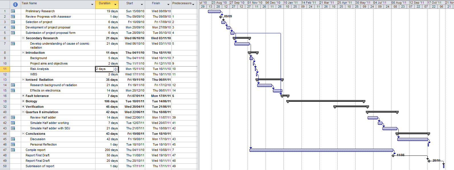
Additional Avionics Research
Aircraft Certification – FAA & EASA
Aircraft equipment can be certified for commercial flight by either by the Federal Aviation Administration (FAA) or European Aviation Safety Agency (EASA).
The D0-178B is the standard for developing avionics software-intensive systems jointly prepared by the Radio Technical Commission for Aeronautics (RTCA). This standard is the collective agreement on how to build reliable software and has been validated over several years in industry.The D0-178B defines specific level of safety criticality from highest to lowest, which are shown in Table B‑1.
|
Software Level |
Failure Condition |
Failure condition interpretation in the Aircraft / Aviation context |
|
A |
Catastrophic |
prevent continued safe flight or landing |
|
B |
Hazardous / Severe-Major |
potential fatal injuries to a small number of occupants |
|
C |
Major |
impairs crew efficiency, discomfort or possible injuries to occupants |
|
D |
Minor |
reduced aircraft safety margins, but well within crew capabilities |
|
E |
No Effect |
does not affect the safety of the aircraft at all |
Table ‑ DO-178B criticality table [D0-178B]
Once the supplier has designed and developed a product for Avionic use, the unit will be subjected to qualification testing as detailed by the customer requirements. Depending on whether the product is intended to be used in Europe or America, the product can then be assessed and accredited with EASA or FAA approval respectively. Providing a hardware change does not impact the form fit function of the unit, EASA or FAA approval may not be required. However, all software changes require re-accreditation. As part of quality control it is also mandatory that the products part number should change to give visibility and tractability of the change. This means that by looking at the part number printed externally on the products nameplate, you know which software is installed.


Correspondence
Correspondence from NASA discussing ionised radiation.
Radiation hardened FPGAs
Data was collected from state-of-the-art FPGAs to determine the level of total dose radiation their products can withstand, and this is shown in Table B‑2. The data tells us that a tolerance of 300K rad, or greater is a common place. These ionised radiation levels are what manufactures are targeting their FPGAs to withstand without permanent damage. These FPGAs are also targeted for space flight which is going to be subjected to a significantly higher dose of radiation compared to commercial flight. A range of suppliers for Actel and Xilinx have been approached, but it has not been possible to obtain any quotations within the times scales for this case study. A search online has not revealed any prices either. It is believed this is because of the specialised nature of the device.
|
Manufacturer |
PN |
TID; Latch up |
|
Atme |
TSC695F |
>300K rad |
|
Atme |
TSC695FL |
>300K rad |
|
Atme |
AT697E |
>200K rad |
|
Atme |
AT697F |
>300K rad |
|
Actel |
RH1020 |
300K rad |
|
Actel |
RTAX250S/SL |
300K rad |
|
Actel |
RTAX1000S/SL |
300K rad |
|
Actel |
RTAX2000S/SL |
300K rad |
|
Actel |
RTAX4000S/SL |
300K rad |
|
Xilinx |
XQR4VLX200 |
300K rad |
|
Xilinx |
XQR4VSX55 |
300K rad |
|
Xilinx |
XQR4VFX60 |
300K rad |
Table ‑ List of Radiation Hardened FPGAs
Additional Biological Research
This is a continuation of Section 4, and provides further breakdown of the Eukaryote structure.
Eukaryote cells
This section provides a more in-depth review of the Eukaryote cells.
Plasma membrane
The plasma membrane is a biological membrane which partitions the contents of a cell from the outside. The membrane is semi permeable allowing the control of cellular movement entering and exiting the cell. The membrane also forms part of the intracellular cytoskeleton which allows the structure of the cells to become formed.
Lysosome
Lysosomes organelles have the function of autolysis, which is to self-digest. This is achieved by the enzymes contained within the lysosome allowing cellular debris degraded organelles, food particles and endocytized materials to be bio-degraded.
Golgi Apparatus
The golgi apparatus has the function of organising, modifying and packaging macromolecules for use within the cell. The macromolecules can also be cell secreted for use outside of the cell. It also transports lipids around the cell and creates lysosomes.
Secretory Vesicle
The Secretory Vesicle is small membrane enclosed sacs which are used to store hormones and neurotransmitters. These sacs are derived from the Golgi apparatus and its function is transfer materials to the cells surface and perform exocytosis, where the materials are exported through the cells plasma membrane to the outside environment.
Smooth Endoplasmic Reticulum
The smooth endoplasmic reticulum is a vast network of membrane bound vesicles and tubes and is part of the outer nuclear membrane. It functions is dependent on the specific type of cell, including synthesis of lipid and steroids, and control of calcium release. It works in conjunction with the Golgi apparatus, Ribosome’s, RNA, mRNA & tRNA.
Ribosome’s
The ribosome is components of the cells that transcribe DNA amino acids into RNA, and then RNA into proteins.
Cytoplasm
The cytoplasm is the fluid that fills the cells.
Nuclear Pore
The membrane encapsulating the nucleus is performed with holes known as Nuclear Pores, this is shown in Figure B‑4. These pores allow the transportation of molecules between the nucleus and the cytoplasm. An example is where the nuclear pores only allow proteins to enter should they contain the correct nuclear localisation signals. In addition RNA transcribed in the nucleus and proteins which are to be exported to the cytoplasm are tagged with nuclear export sequences for release through the nuclear pores. (56)
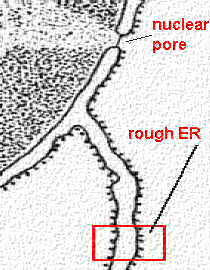
Figure ‑ Nuclear Envelope (57)
Nuclear Envelope
The nuclear envelope consists of two membranes covered in nuclear pores. This membrane acts as a physical barrier to the nucleus.
Nucleus
The nucleus contains the majority of the cells genetic material. Its function is to maintain the integrity of the genes. The nucleus assists in the control of cell movement, reproduction, and regulation of food.
Prokaryote and Eukaryote Energy
Both eukaryote and Prokaryote cell organisms obtain energy from cellular respiration which has three main stages.
- Glyrolysis. Metabolic pathway that converts glucose C6H12O0 into pyruvate acid CH3COCOO−
- Citric Acid Cycle. A reaction which occurs in the mitochondrion part of the metabolic pathway. This involves chemically converting carbohydrates, fats and proteins into carbon dioxide and water
- Electron transport. A reaction between electron donor and an electron acceptor across a membrane
POEtic Model
POEtic systems are inspired by three biological features Phylogenesis (P), Ontogenesis(O) and Epigenesis (E).
Tyrell (49) describes the POE model as having a common basis for the Genome. Phylogenesis is the history of the species evolution. Ontogenesis is the development of an individual as orchestrated by its genetic code. Epigenesis is the development of the individual through the learning process which is influenced by the genetic code and the environment. Tyrell reports that a bio-inspired systems requires the following basic features:
- Re-configurability
- Multi-cellular scalable structure
- Possibility of implementing POE in any combination or separately in a layered approach
- Massive I/O interaction with the external environment
Whilst classic hardware may not be typically utilise dynamic routing, this is essential for an ontogenetic and epigenetic mechanism.
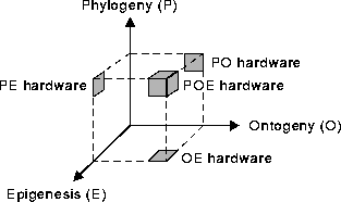
The embryonic cells discussed in the previous chapter are very complex, and the limitations in modern fabrication techniques are not comparable since the FPGA silicon cannot self-replicate.
However, the four important characteristics can be learnt from the cell which should be considered when designing the embryonic cell.
- Each cell is self-contained with its own instructions. The cell can operate independently amongst other cells
- The cell can decide when to self-terminate
- No single cell is critical to the completion of the task
- The cell has a layered / modularised approach. Each part of the cell has a function and together completes the main objective for which it is programmed.
Additional Systems Research
Column Elimination
This is a demonstration of column elimination. This works by replacing a faulty cell with a new column of cells.


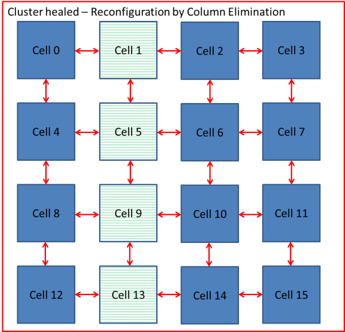
Figure ‑ Reconfiguration by Column Elimination

Initial Designs VHDL Designs
This section shows one of the initial ideas the development states of the project, was to create a robust Logic gate using TMR with the ability to inject SEU faults. However, this did not use any inspiration from a biological cell, and therefore these designs were not used in the final embryonic cell as they were replaced by the logic unit and Genome and shown here for illustration purposes only.
Logic AND gate with built in SEU testability
Initial design at the start of project to create a robust AND gate using TMR with the ability to inject SEU faults. This was not used in the final design.
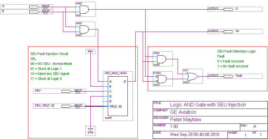
Figure ‑ Initial Logic AND gate with built in SEU testability
Initial Logic OR gate with built in SEU testability
Initial design at the start of project to create a robust OR gate using TMR with the ability to inject SEU faults. This was not used in the final design.
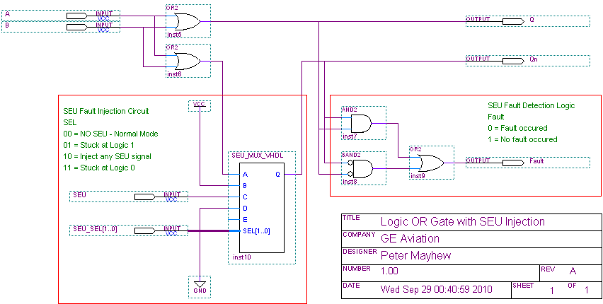
Figure ‑ Initial Logic OR gate with built in SEU testability
Initial Logic NOT gate with built in SEU testability
Initial design at the start of project to create a robust NOT gate using TMR with the ability to inject SEU faults. This was not used in the final design.

Figure ‑ Initial Logic NOT gate with built in SEU testability
Logic XOR gate with built in SEU testability

Figure ‑ Initial Logic XOR gate with built in SEU testability
Single Event Effects
This section provides a comprehensive list of SEE types.
Multiple Bit Upset
Multiple Bit Upset (MBU) is where a single ionised particle passes through an electrical device causing multiple upsets or transients as the particle passes through the semiconducting material. The scale of the updates would depend on the architecture of the system.
Single Event Functional Interrupt
Single Event Functional Interrupt (SEFI) was first documented in the 1996 issue of EIA/JEDEC standard and is where a single ionised particle can cause temporary non-functionality of the effected device (58). SEFI may last as long as the power is maintained, or it can last for a finite period. An example of such a failure would be a SEU corrupting the devices control path which would result in a lock-up condition. (4)
Single Event Latch-up
Single Event Latch-up (SEL) is a condition where the ionised particle impacts the CMOS device and the localised energy induced into the material causes parasitic transistors to be switched on, resulting in high power supply currents. After contacting NASA Electronic Parts and Packaging Program it was confirmed that SEL is defined as being potentially destructive (Appendix B.2, reference Email from NASA). This type of failure can only be resolved by cycling the power to the system.
Single Event Transient
Single Event Transient (SET) is a result of heavy ions or a high energy proton impacting a sensitive area on an IC resulting in current spikes on transistor terminal that can propagate through the IC. Depending on the application of the device, SET can be non-destructive or can cause permanent failure (59).
Single Hard Error
A Single Hard Error (SHE) causes a permanent change to the operation of the semiconductor, for example causing a stuck bit in a memory device. This type of condition is typically caused by heavy ions.
Single Event Burnout
Single Event Burnout (SEB) is a destructive event in high voltage devices such as N Channel MOSFETs, BJO, GTO thyristors, power diodes, and IGBTs. This condition occurs when a ionised particle creates a transient current whilst the device is in the off state. This causes a regenerative feedback loop which exceeds the breakdown voltage (4).
Single Event Gate Rupture
Single Event Gate Rupture (SEGR) is a destructive event when a heavy ion impacts the device causing the dielectric on the gate insulator to breakdown. For example, an EEPROM during the erase or write sequence is driven at a higher voltage, and the heavy ion can cause a local breakdown of the insulating silicon dioxide, another example would be with high voltage MOSFET’s.
SRAM based FPGA susceptibility to ionised radiation
The key components which are susceptible to atmospheric radiation effects have been categorised by GE Aviation, shown in Table D‑1.
Table ‑ Component Types and SEE Susceptibility (4)
The volatile memory on SRAM, DRAM and SDRAM in FPGA are susceptible to SEE, and the types of SUE failure rates are shown in Table D‑2.
Table ‑ Volatile memory SEE failure rates (4)
Boron-10 is present in devices with Borophosphosilicate glass passivation (BPSG). BPSG is used as part of the devices fabrication for insulating layers, the scaling factor in Table D‑2 should be used (4). This is a result of Boron-10 isotope capturing thermal neutrons from ionising radiation.
Error Detection Code
The techniques discussed in this section enable a system to automatically detect whether data contains an error.
Parity Check
Parity checking is used to verify the data symbol has been correctly transmitted. It uses a parity generator circuit which produces either an even or odd parity bit (decided by the user). This parity bit is transmitted along with original symbol. Parity checking allows us to detect a single bit flip. It cannot detect two bit flips, or correct the code (60).
Checksums
The checksum is a special code derived by adding up the data words stored in all memory locations. The checksum is then added to the end the memory location. A separate system can then reading back the data words and generating its own checksum. A difference in the checksum values will indicate the data has changed. However, the exact location of the error cannot be determined (60).
Cyclic Redundancy Check
A Cycle Redundancy Check (CRC) is a hash function, and is designed to detected changes in data. Each memory frame has an associated CRC value which is stored in memory. The Los Alamos National Laboratories Space Data Systems Group developed a read-back verification algorithm. The algorithm performs a read-back of the memory and generates a CRC value for each frame. If the system detects a difference between the CRC value generated and that which is stored in memory, the frame number is recorded and corrected once the read-back process is complete.
A report by Xilinx (61) states that it is unlikely more than one SEU will be detected. However, it is recommended that a system is designed to accommodate the detection of more than one SEU. This can be achieved by allocating enough memory to log multiple corrupted frame numbers.
Configuration data scrubbing
Data scrubbing is a process where the memory frames in the FPGA are read and their contents verified by comparison to another source. It is common practice for memory scrubbing systems use Single Error Correction Double Error Detection (SECDED) (38). This is Hamming code; another method would be to embed Cycle Redundancy Checks (CRC). The Limitation of SECDED is that two errors can be detected, but only one error corrected. Scrubbing prevents the accumulation of configuration upsets, and reduces the probability that two SEUs will compromise a DMR or TMR system. SRAM based FPGA are manufactured in standard device memory sizes and the configuration memory might only require 10% to define the logic. Therefore the error rate is lower that the upset rate of the SRAM.
There are two forms of scrubbing, and this is Blind Scrubbing & Read-back Scrubbing.
Blind Scrubbing
Blind Scrubbing utilises external memory which contains a copy of the original configuration data. The scrubber copies each frame from the external memory, and overwrites the data stored in SRAM configuration data. In order for this design to function correctly the external memory will also need to be tolerant to SEUs.
However, because the blind scrubber simply over writes all frames, there are no means to detect or report corrupt frame(s). A more complex solution is to use read-back scrubbing.
Read-back scrubbing
Read-back scrubbing over writes the configuration data only if a SEU is detected, this will come at the expense of increased complexity of the design. There are a number of different techniques for read-back scrubbing using a combination of Error Code Correction (ECC) and original data stored in external memory. To perform read-back scrubbing a dedicated configuration controller circuit is required. The configuration controller can be external to the FPGA using a dedicated radiation hardened controller circuit as shown in Figure D‑8. A paper by Heiner (38) suggests that the configuration controller can also be internal to the FPGA as shown in Figure D‑9. Whilst memory scrubbing does provide advantages, it is not possible to perform this whilst partial reconfiguration is in progress. This is because partial reconfiguration will require write access to the configuration data, whilst memory scrubbing will require read and write access to the configuration data. Therefore, a protocol will be required for these two techniques to co-exist simultaneously, without the risk of corrupting configuration data. A solution would be to inhibit the scrubber whilst partial configuration is in progress.
Figure ‑ Overview of single FPGA, in Master SelectMAP Mode, Self-Hosting a Triplicate Configuration Management (62)
Figure ‑ Read-back with CRC scrubbing architecture (38)
Additional Verification Test
The section shows some of the tests performed to verify the embryonic cell could perform a fundamental operations such as LOGIC AND, OR and NOT function.
Logic OR Gate Verification
First, the embryonic cell was configured to operate as a Logic OR gate. The simulated waveform shown in Figure E‑1 demonstrates the Genome can correctly configure the cell to operate as a Logic OR gate.
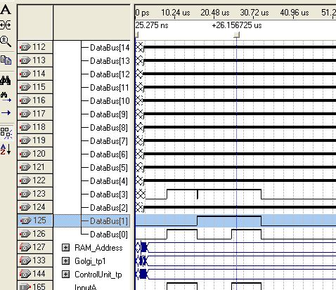
Embryonic Cell Inputs
Embryonic Cell Output
Figure ‑ Cell Verification – Logic OR Function
Logic NOT Gate Verification
The simulated waveform in Figure E‑1 demonstrates a single cell operating as a Logic NOT gate. Therefore, this confirms the Genome can correctly configure the cell to operate as a Logic NOT gate.

Embryonic Cell Input
Embryonic Cell Output
Figure ‑ Cell Verification – Logic NOT Function
Verification of Genome Loaded into Cluster
This section demonstrates the 32-bit Genome being loaded into the cluster which is used to configure all the required cells. Each cell will read the Genome, determine an unallocated function and attempt to take ownership of that function. Although a 32-cell cluster could not be simulated in this project due to the limitation of logic element, this shows the Genome already designed for a 32-cell cluster.
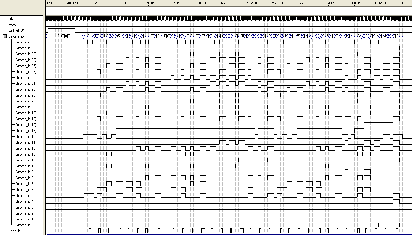
Figure ‑ Loading Genome into Cluster
VHDL Design issues – Root Cause Analysis
During development there were several design issues VHDL design which required root cause analysis and a design solution.
Several tools are available for root cause analysis such as 5 Whys, decision tress, 8D reports, and Apollo RCA. It was decided that Apollo RCA would be the most appropriate for this issue since it can be used generally for any problems and defines both the problem cause / effect.
Two particular issues successfully diagnosed shall be discussed.
Embryonic Cell – Databus Corruption Bug
After designing the first embryonic cell, its functionality was verified and confirmed to operate correctly as shown in Section 6.However, as the embryonic cells were connected the tests revealed that the cluster would occasionally produce undefined outputs as shown in Figure E‑4.
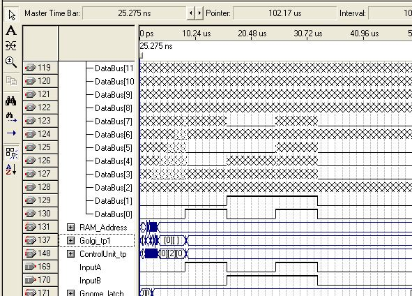
Embryonic Cells with undefined outputs
Figure ‑ Example of Bug causing undefined outputs
To resolve this issue an Apollo Root cause Analysis chart was used. This uses the principle that for every action, there is a conditional cause and action cause.
Figure ‑ Framework for Apollo Root Cause Analysis
This process was used to determine the root cause of the cluster not working.
Root cause
When the cells are first initialised the RAM is not configured and therefore outputs are in an indeterminate state. Each cell assigned a function then configures it’s the RAM to defined output. However, any unused cells are still left in an indeterminate state and therefore its outputs are undefined. The unknown outputs are then fed into the latch, which is sent to the logic unit. The result is corruption on the data bus
The resolution was to initialise the first memory location in RAM to a predefined value.
Steps to resolve
- Enter Control unit State 1
- Output predefine value to RAM
- Move to Control unit state 7. Update RAM memory location. Reset memory address pointer
- Return to Control Unit state 2
- Continue as normal
The cluster was re-tested and the data bus was not corrupted. This successfully resolved the software bug.
Embryonic Cluster – Cells 13-16 not working
Earlier in the project development it was possible to simulate up to a 16 cell cluster as the number of logic element did not exceed the FPGA specification. (As the embryonic cell developed due to bug corrects, it was no longer possible to fit more than 12 cells on the FPGA).
The verification tests initially started with verifying a single cell, then a cluster of 2,4,8,12 cells. The clusters operated as expected. However, simulating 16-cells shows that cells 13-16 (last four cells in the cluster) were not providing the expected output response.
The cell diagnostic test outputs were monitored to confirm the operation of the Golgi apparatus and control unit state machines.
Analysis found databus bit 15-18 were not responding as expected. Cells 13-16 when then reconfigured using the Genome to output on database bits 24-27. Cells 13-16 outputs were now as expected.
A test signal was then sent into each databus bit 0-31 and the results are shown in Figure E‑6. The results show that databus bits 15-16 produced an invalid output response.
Root cause
The root cause was due to two transposed signals on MUX 1 in the logic unit.
Steps to resolve
The transposed signals were corrected and verified that databus bits 15-16 could produce the correct output response.
Once this fix was implemented, it was no longer possible to fit a cluster of 16-embryonic cells on a FPGA due to exceeding the available logic element available on the device. In-stead the maximum number of embryonic cells that could be simulated was 12. This was not a particular concern as the project could still be validated a success by simulating a half adder which only required 6 embryonic cells.
|
Databus bit |
Pass/Fail |
Databus bit |
Pass/Fail |
Databus bit |
Pass/Fail |
Databus bit |
Pass/Fail |
|
0 |
Pass |
9 |
Pass |
18 |
Pass |
27 |
Pass |
|
1 |
Pass |
10 |
Pass |
19 |
Pass |
28 |
Pass |
|
2 |
Pass |
11 |
Pass |
20 |
Pass |
29 |
Pass |
|
3 |
Pass |
12 |
Pass |
21 |
Pass |
30 |
Pass |
|
4 |
Pass |
13 |
Pass |
22 |
Pass |
31 |
Pass |
|
5 |
Pass |
14 |
Pass |
23 |
Pass |
||
|
6 |
Pass |
15 |
Fail |
24 |
Pass |
||
|
7 |
Pass |
16 |
Fail |
25 |
Pass |
||
|
8 |
Pass |
17 |
Pass |
26 |
Pass |
Apollo root cause analysis
Based on the evidence available an Apollo Reality Chart was generated which gave a structured approach in determining the root cause. The reality chart is shown in Figure E‑7 &Figure E‑8.Figure E‑8
Continue on sheet 2
Figure ‑ Apollo Reality Chart Part 1/2
Root cause
Flow of root cause
Figure ‑ Apollo Reality Chart Part 2/2
Pre- Development work of Half Adder in Excel
Prior designing the Embryonic cluster in VHDL, the theory was written in excel to confirm whether this was a practical solution. This pre-development work is shown below in Table E‑1 & Table E‑2.
|
Signal line |
Logic Gate |
I/O |
Timeslot 1 |
Timeslot 2 |
Timeslot 3 |
Timeslot 4 |
|
1 |
AND 1 |
A |
1 |
1 |
1 |
1 |
|
2 |
B |
0 |
0 |
0 |
0 |
|
|
3 |
Q |
FALSE |
FALSE |
FALSE |
FALSE |
|
|
4 |
AND 2 |
A |
– |
1 |
||
|
5 |
B |
0 |
0 |
0 |
0 |
|
|
6 |
Q |
– |
FALSE |
FALSE |
FALSE |
|
|
7 |
AND 3 |
A |
– |
TRUE |
TRUE |
TRUE |
|
8 |
B |
1 |
1 |
1 |
1 |
|
|
9 |
Q |
– |
TRUE |
TRUE |
TRUE |
|
|
10 |
NOT 1 |
A |
1 |
1 |
1 |
1 |
|
11 |
Q |
FALSE |
FALSE |
FALSE |
FALSE |
|
|
12 |
NOT 2 |
A |
0 |
0 |
0 |
0 |
|
13 |
Q |
TRUE |
TRUE |
TRUE |
TRUE |
|
|
14 |
OR 1 |
A |
– |
– |
FALSE |
FALSE |
|
15 |
B |
– |
– |
TRUE |
TRUE |
|
|
16 |
Q |
– |
– |
TRUE |
TRUE |
Blank Cell finished
Back text Sum
Red text Carry
Grey Output
Table ‑ Half Adder IP Addresses & Time Slots
|
Genome |
||||||||
|
Function |
function to perform |
Allocated |
Timeslot A |
Timeslot B |
Timeslot Q |
IP Address A |
IP Address B |
IP Address Q |
|
1 |
AND1 |
0 |
1 |
1 |
2 |
000000 |
001000 |
011000 |
|
2 |
AND2 |
0 |
2 |
2 |
3 |
010000 |
000001 |
001001 |
|
3 |
AND3 |
0 |
2 |
2 |
3 |
011001 |
010001 |
000011 |
|
4 |
NOT1 |
0 |
1 |
NA |
2 |
001011 |
011011 |
010011 |
|
5 |
NOT2 |
0 |
1 |
NA |
2 |
000010 |
001010 |
011010 |
|
6 |
OR1 |
0 |
3 |
3 |
4 |
010010 |
000110 |
001110 |
Table ‑ Genome Table for Half adder
Two-bit Full Adder
The original aim of the project was to simulate the functionality of a Two-bit adder. A Two-Bit full adder can be designed using a half adder which adds together Two bits, and a full adder which adds together 2 bits and the carry bit. The Two-bit adder can be developed using 25 logic gates. It is important that we note the number of gates required to perform the logic function as each gate shall be replaced by an individual configurable cell in the cluster. For example, if we require a AND gate, one of the cells from the cluster shall be allocated and configured to perform the function of a AND gate, and this would be the same process to perform an OR / NOT logic function.
However, when simulating a 32-cell cluster it become apparent the number of logic elements required during compilation exceed the number of logic elements available on the FPGA, as explained in section 7.5. For illustration purposes only,

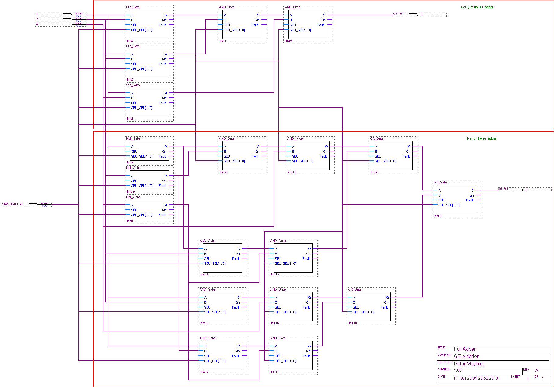
Time Slot 5
Time Slot 3
Time Slot 3
Time Slot 4
Time Slot 4
Time Slot 1
Time Slot 2
Time Slot 0
Time Slot 0
Time Slot 0
Time Slot 0
Time Slot 0
Time Slot 0
Time Slot 0
Time Slot 0
Time Slot 0
Time Slot 0
Time Slot 2
Time Slot 3
Time Slot 0
Time Slot 1
Time Slot 1
Time Slot 2
Time Slot 0
Time Slot 1
Time Slot 0
Time Slot 0
Time Slot 1
Time Slot 3
Time Slot 0
Time Slot 2
Time Slot 2
Time Slot 1
Time Slot 1
Time Slot 1
Time Slot 1
Time Slot 1
Figure ‑ Full Adder Circuit Diagram
Simulated Test Strategy
Testing stage instructions: To validate Embryonic Cell.
Test schedule: 24-06-11 to 24-06-11
Location
Room 3P28
University of West of England
Frenchay Campus
Coldharbour Lane
Bristol
BS16 1QY
United Kingdom
Instructions
Engineering testers
Name: Peter Mayhew Role: Design Engineer / Student
Name: Nigel Gunton Role: Senior Lecturer : Electronics
Testing environment
Equipment required for test
1 x Computer running Windows XP
1 x Quartus ii web edition software
1 xNIOS Demonstration board
1 xByte Blaster cable
1 x Oscilloscope & x10 probe
Preparation
Preload VHDL using quartus ii software to NIOS demonstration board using byteblaster.
Method of testing
Physical input using buttons on NIOS demonstration board to exercise software state machines. The tests performed shall exercise the input of a Genome and whether the cluster has successfully configured to perform the desired function.
Test sheet for Embryonic Cluster
|
TEST SHEET |
|
|
|
|
|
|
Project |
Embryonic Cluster |
|
|
|
|
|
Date |
24-06-11 |
|
|
|
|
|
Engineer |
Peter Mayhew |
|
|
|
|
|
Role |
Design Engineer |
|
|
|
|
|
Engineer |
Nigel Gunton |
|
|
|
|
|
Role |
Senior Lecturer : Electronics |
|
|
|
|
|
|
Para |
|
Pass |
Fail |
|
|
|
1.1 |
Control Unit Module State Machine Test |
|
|
|
|
|
1.2 |
Golgi Apparatus State Machine Test |
|
|
|
|
|
1.3 |
RAM Controller State Machine Test |
|
|
|
|
1.4 |
RAM State Machine State Machine Test |
||||
|
1.5 |
IP Address Generator State Machine Test |
||||
|
1.6 |
TimeSlot Generator State Machine Test |
||||
|
1.7 |
Logic Unit VHDL Test |
||||
|
1.8 |
Single Cell Test |
||||
|
1.9 |
Cluster of 12-Cells Test |
||||
|
2.0 |
Cluster detects Simulated SEU |
||||
|
2.1 |
Cluster recovers from Simulated SEU |
||||
|
|
|
|
|
|
|
|
|
Software version tested: |
|
Version 1.4 |
||
|
|
Engineer 1 Signature: |
|
PJM |
||
|
|
Engineer 1 Date: |
|
02-02-11 |
||
|
|
|
This software has been tested and verified to have : |
|
PASSED/ |
|
Circuit Diagram
This section shows the circuit diagrams and flow charts for the biologically inspired design. The circuit diagrams are screen shots taken from Quartus ii. circuit diagrams for each module and also the complete cluster design is included. In addition the 16-cell and 32-cell cluster circuit diagram is shown, which could not be simulated due to the lack of logic elements available.
Golgi Circuit Diagram
Embryonic Cell Circuit Diagram

Figure ‑ Embryonic Cell Schematic
RAM Controller Circuit Diagram

Figure ‑ RAM Controller Schematic
Logic Unit Schematic Circuit Diagram
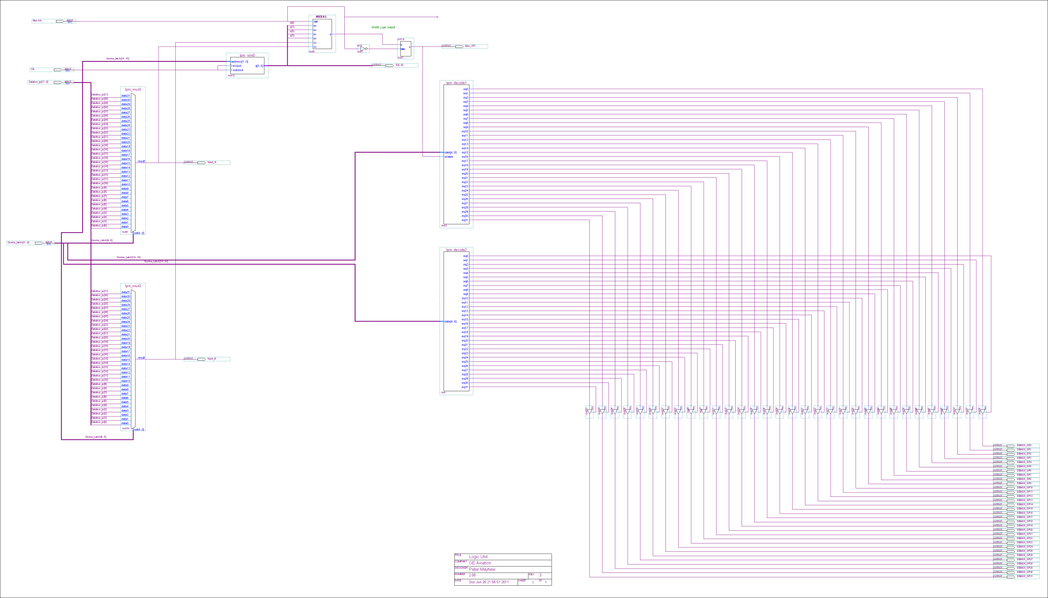
Embryonic Cell (First) Circuit Diagram
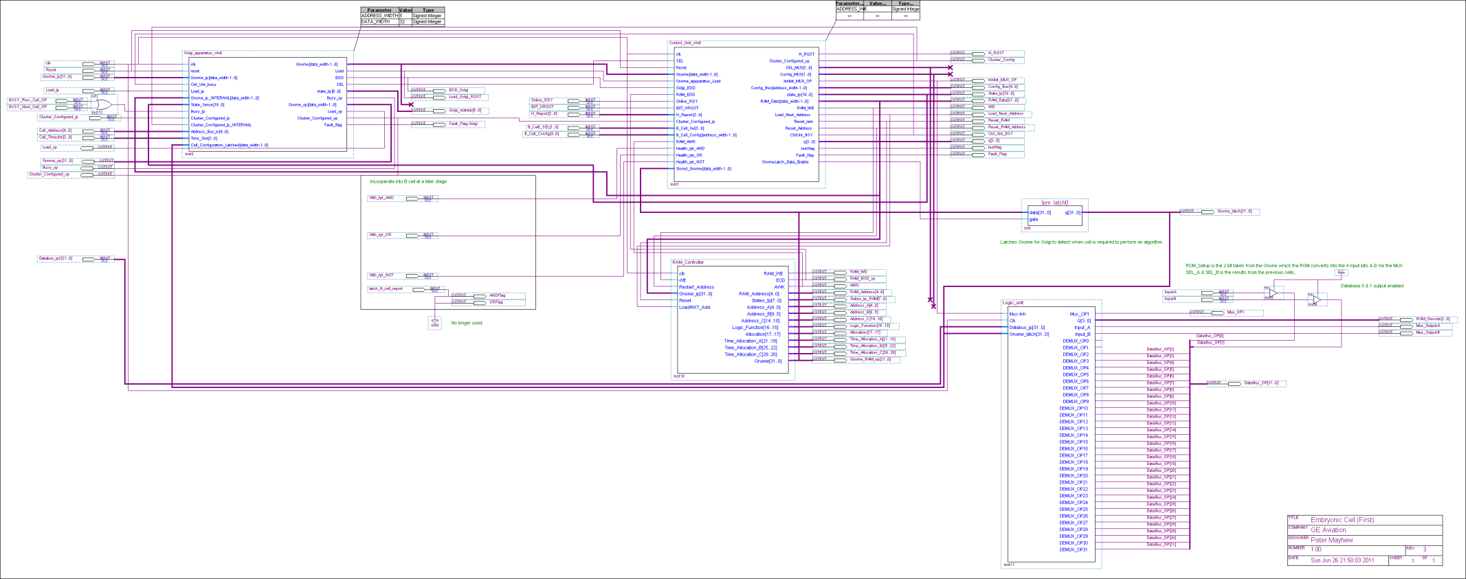
Figure ‑ Embryonic Cell (first cell) Schematic
Embryonic Cell Circuit Diagram
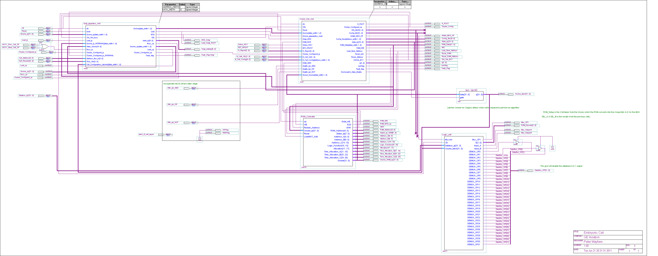
Figure ‑ Embryonic Cell Schematic
Cluster of 4 Embryonic Cells Circuit Diagram
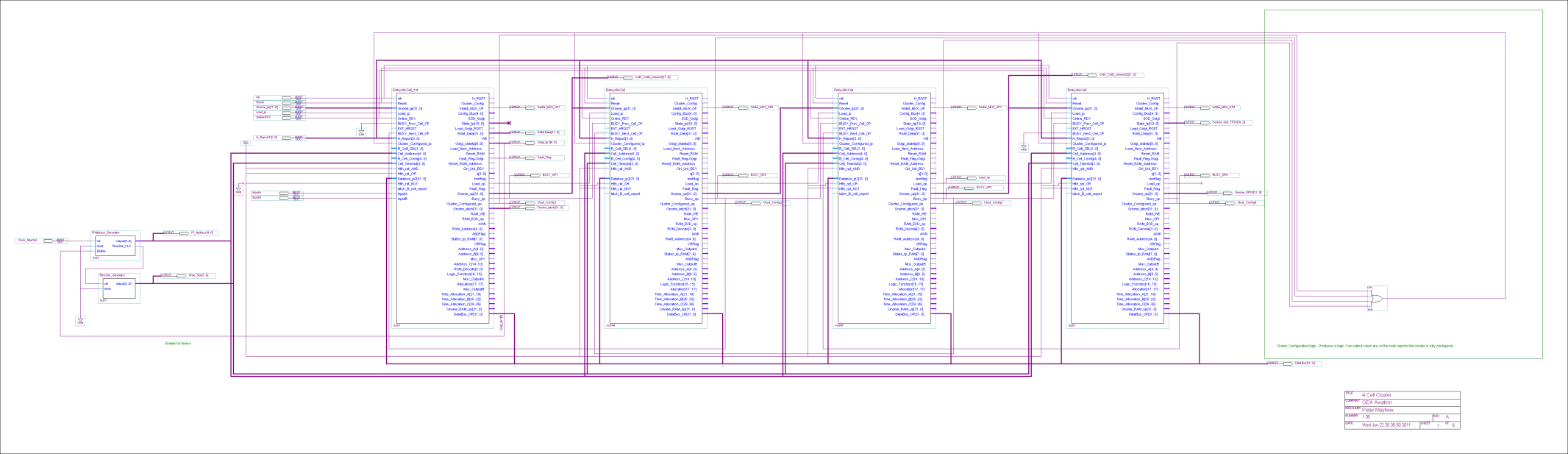
Figure ‑ Cluster with 8 embryonic Cells Schematic
Cluster of 8 Embryonic Cells Circuit Diagram

Figure ‑ Cluster with 8 embryonic Cells Schematic
Cluster of 12 Embryonic Cells Circuit Diagram

Figure ‑ Cluster with 12 embryonic Cells Schematic
Cluster of 16 Embryonic Cells Circuit Diagram
The 16-cell cluster was designed. However, it was not possible to simulate due to a lack of logic elements available on the FPGA used.

Figure ‑ Cluster with 16 embryonic Cells Schematic
Cluster of 32 Embryonic Cells Circuit Diagram
The 32-cell cluster was designed but it was not possible to simulate due to a lack of logic elements available on the FPGA used.

Figure ‑ Cluster of 32 Embryonic Cells
Flow Charts
Golgi Apparatus Flow Chart
This includes a flow chart for two of the Golgi Apparatus states. The reader should be aware that due to the complexity of the design it was agreed with the supervisor that these will be the only two state flow charts included in this report. The reader may find a summary of all the states in section 5.8.
Figure ‑ Golgi Apparatus State 0
Figure ‑ Golgi Apparatus State 1
System Flow Chart. Cluster Configuration
Figure ‑ Cluster Configuration Flow Chart
System Flow Chart – Performing Function
Figure ‑ Cluster Processing Input X & Y Flow Chart
VHDL Source Code
Control Unit VHDL
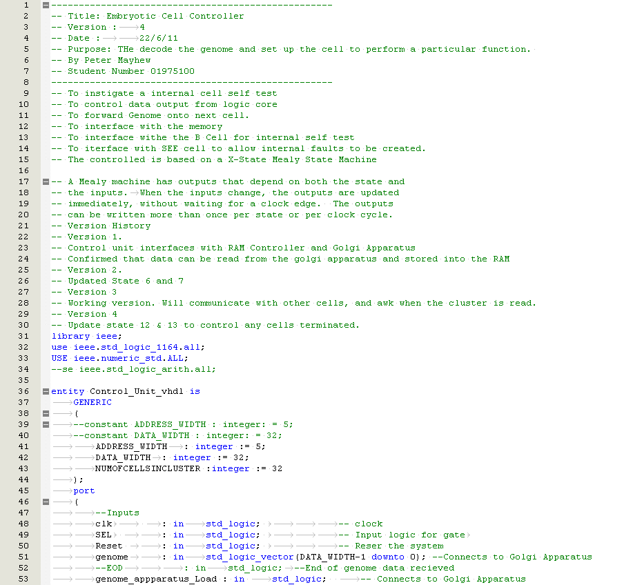
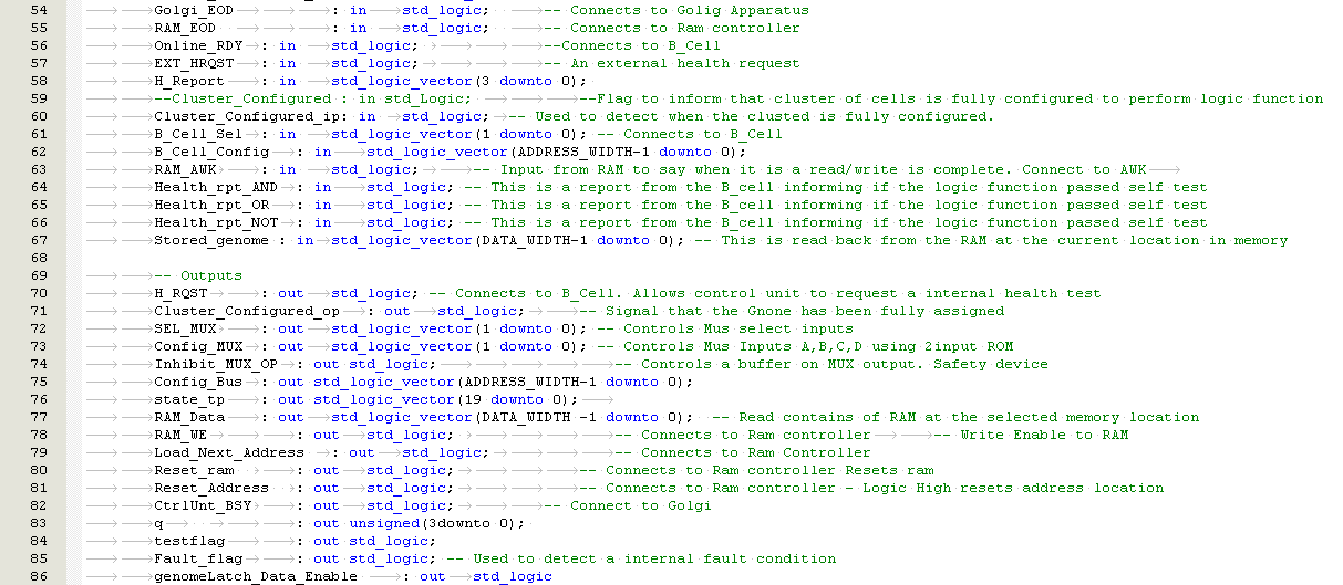

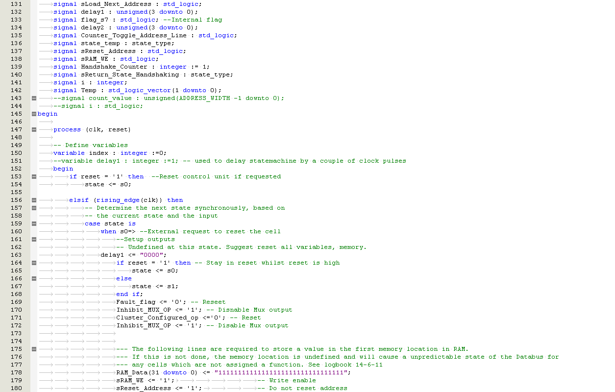

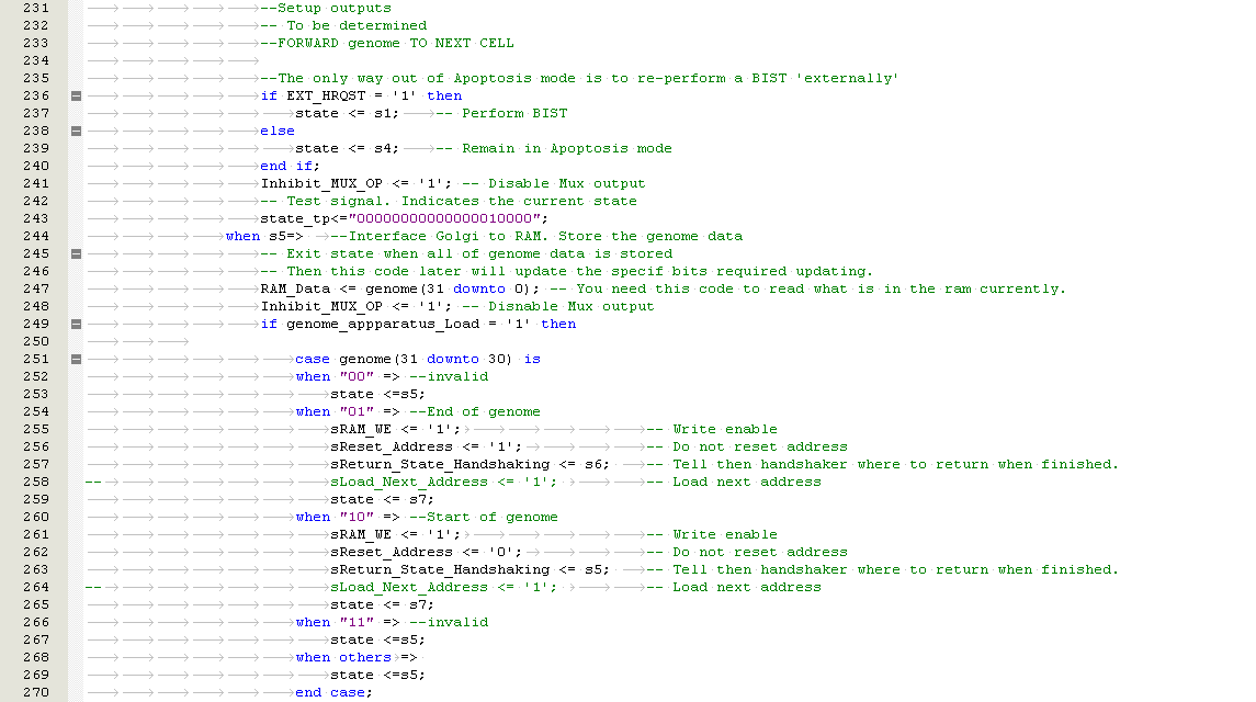

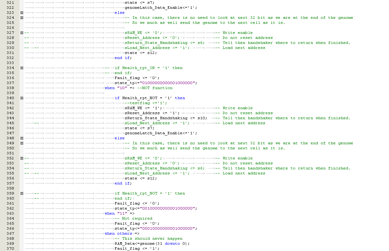
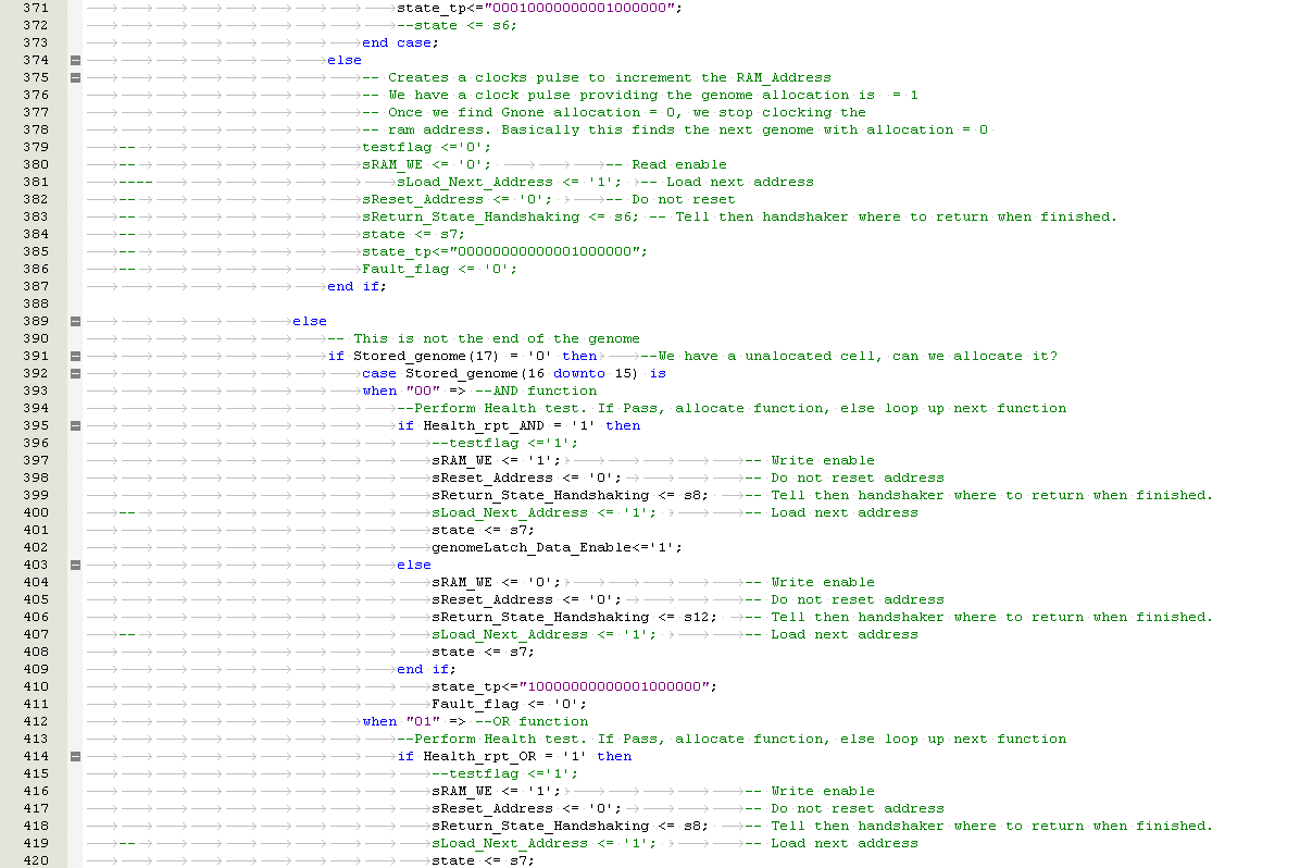
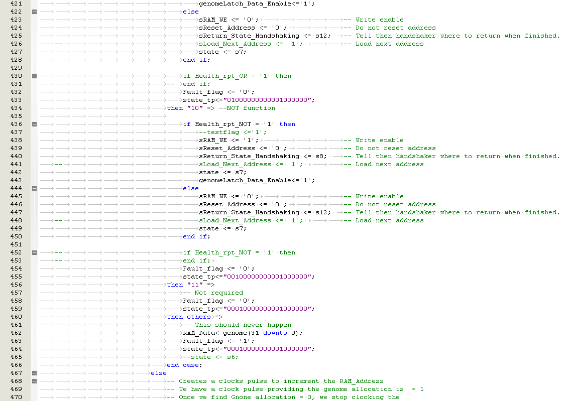
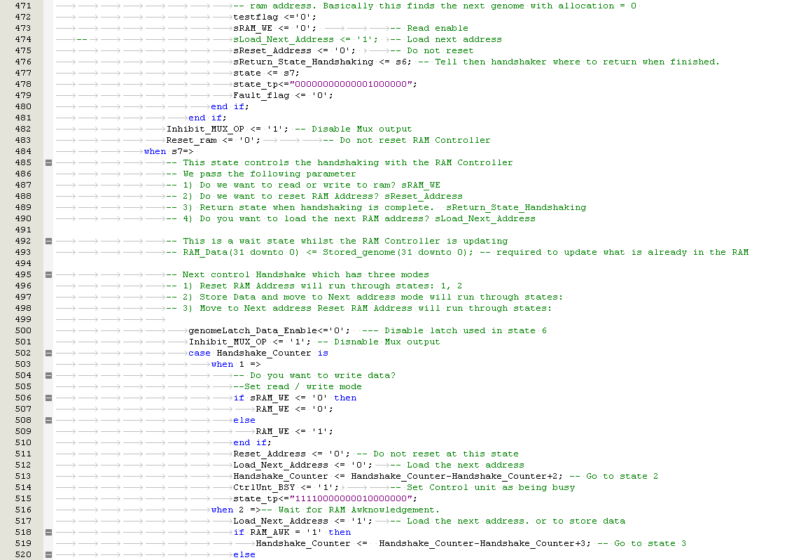
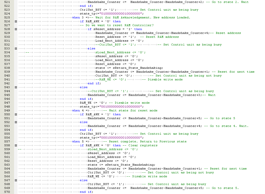


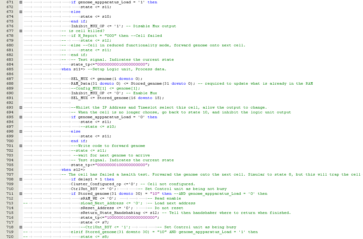
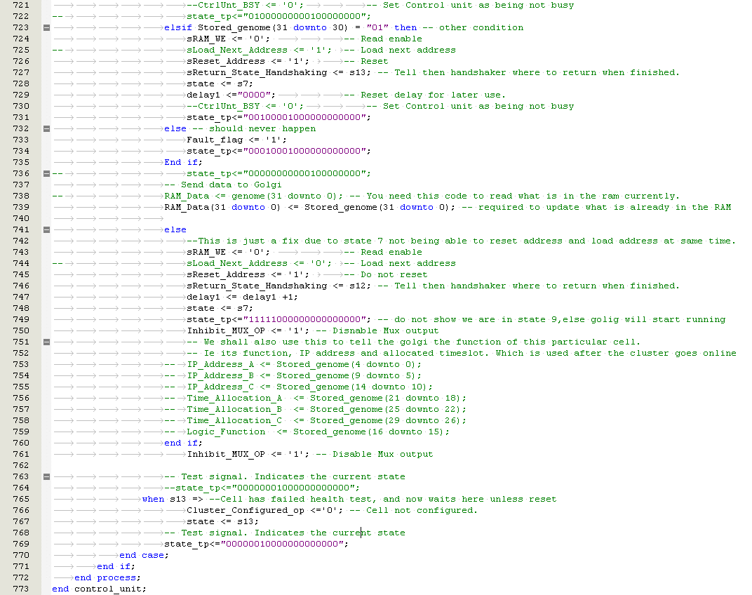
Golgi Apparatus VHDL
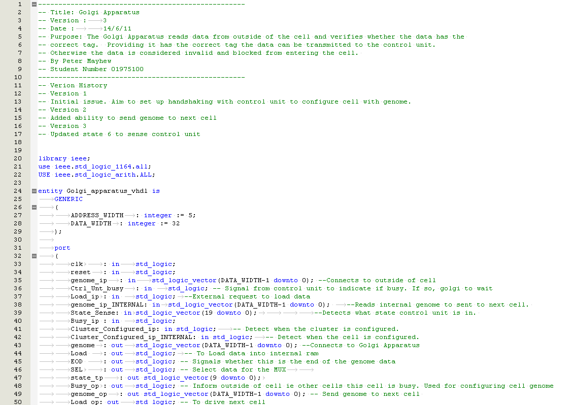
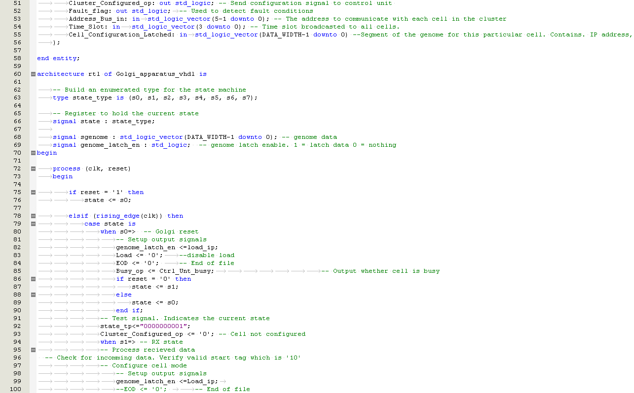
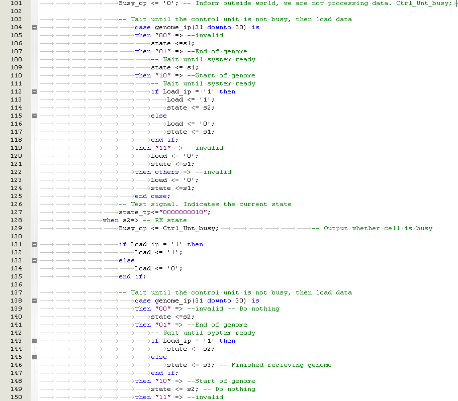


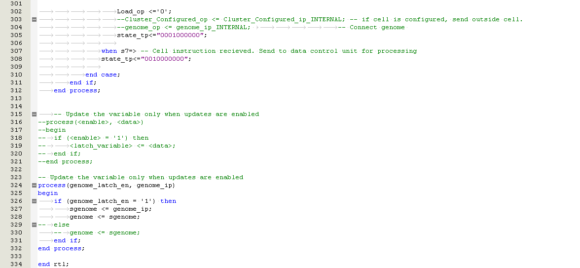
RAM Controller VHDL
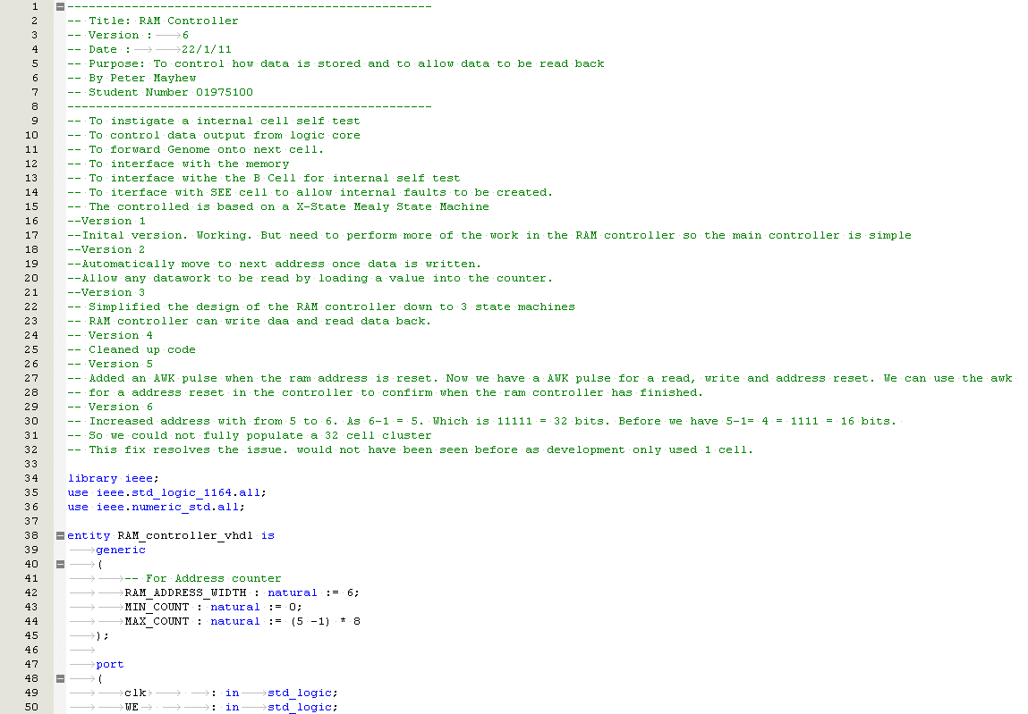
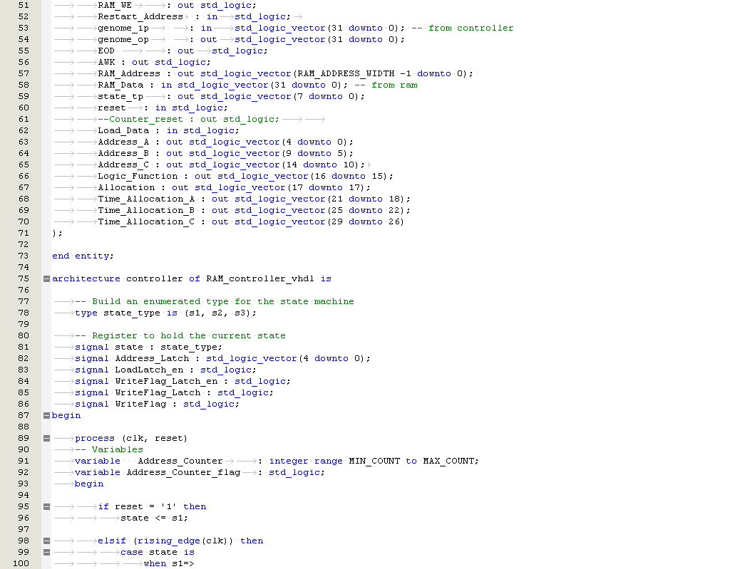
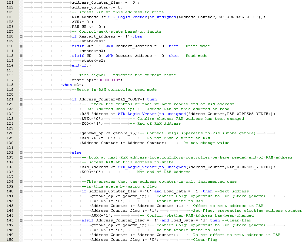
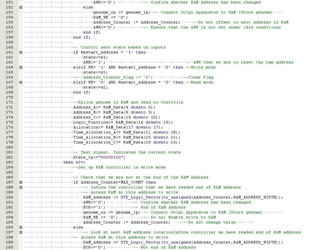

RAM VHDL
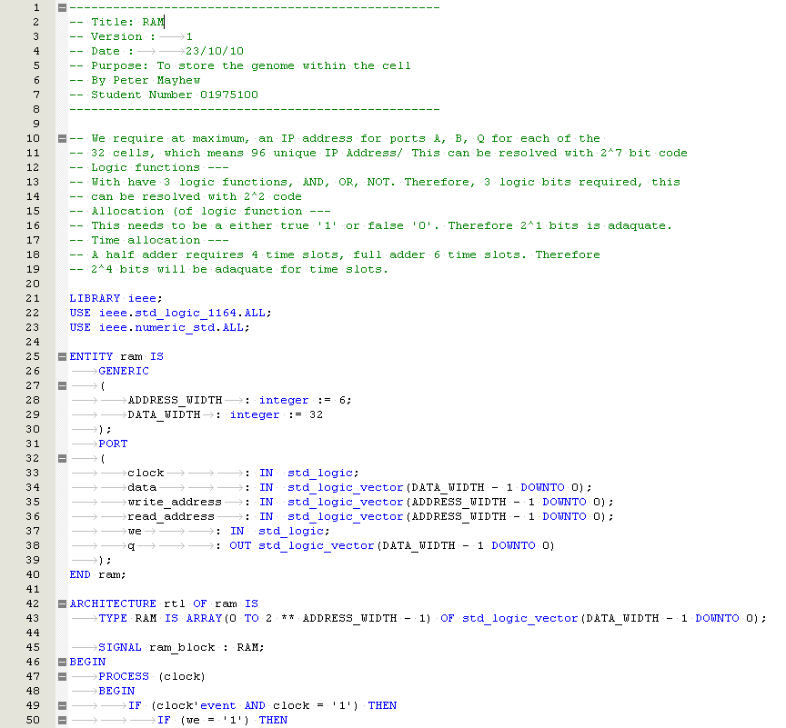
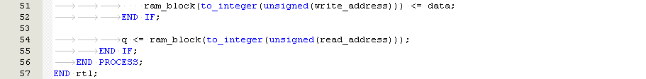
IPAddress Generator VHDL
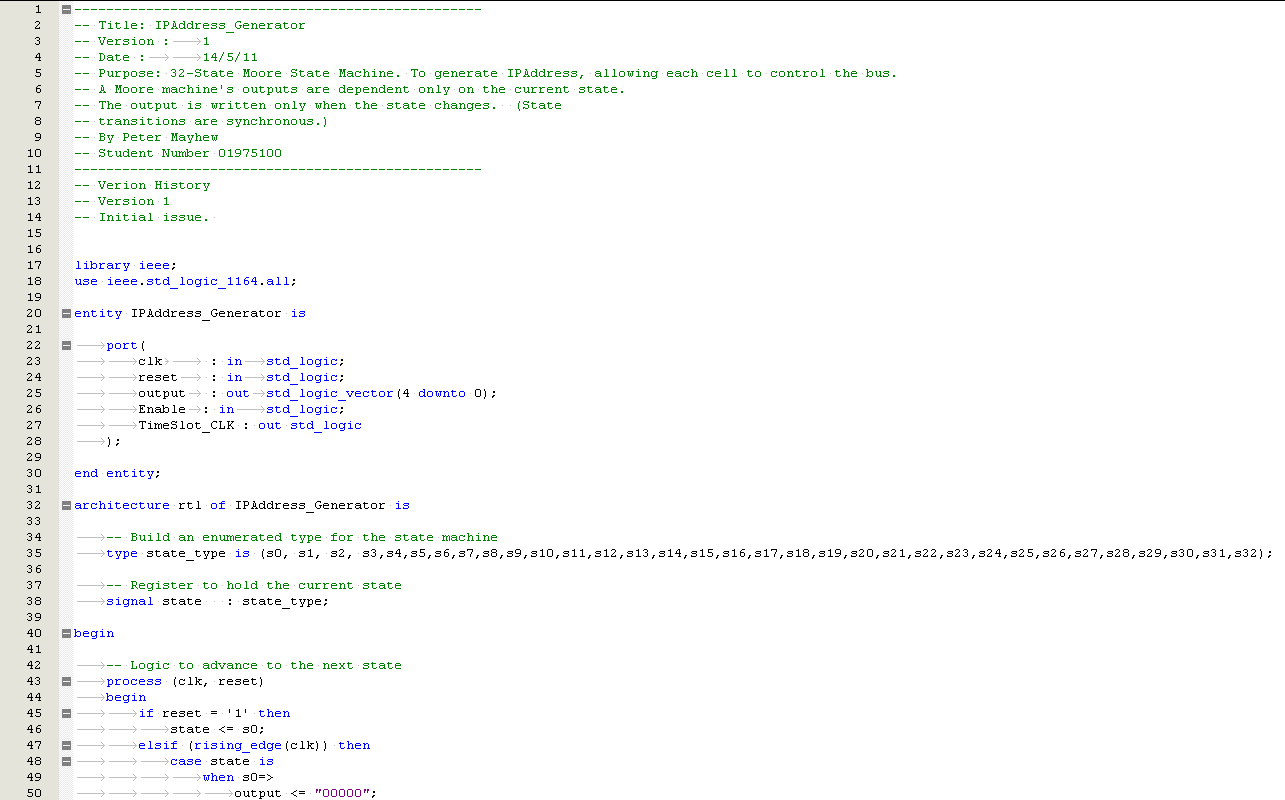

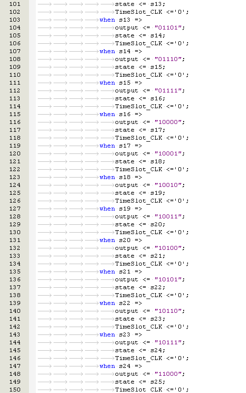
TimeSlot Generator VHDL
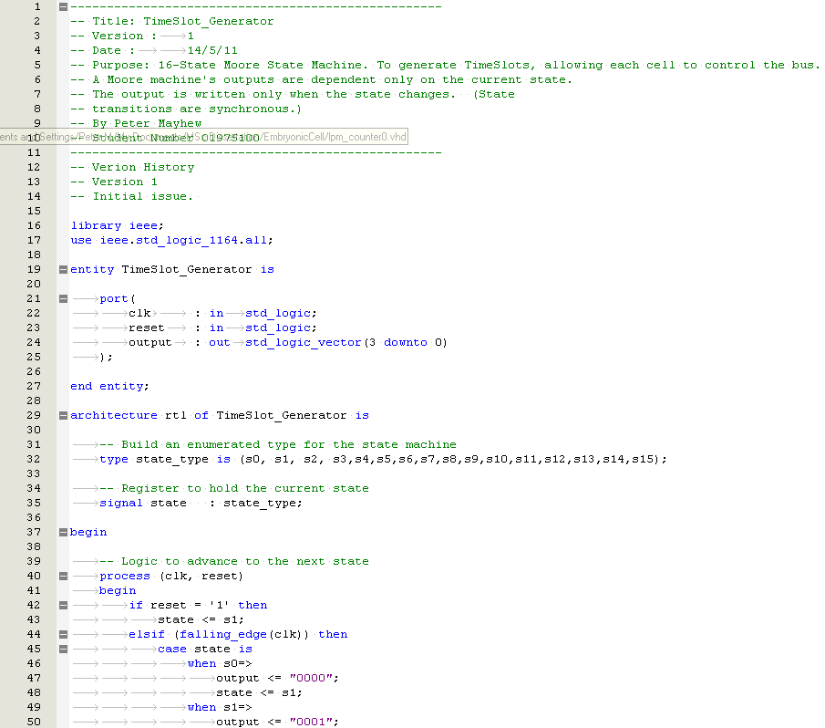
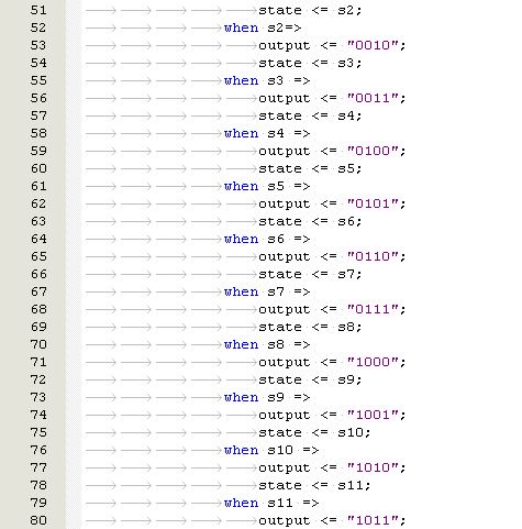
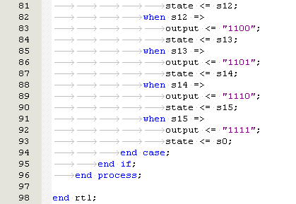
Recent Comments