By Peter Mayhew
Date: 28 May 2001
Summary
-
- This projected involves designing and building a Infra Red remote Control system, to switch On or Off up to eight systems, such as a Fan, Light etc. The project was designed from ‘scratch’ using just TTL Logic ICs.
- The end Project was successful in transmitting data reliably to control up to 8 systems; But was not able to sustain a distance between the Transmitter and Receiver beyond 150mm. This was due development time required and cost implications.
Introduction
-
- As part of my HNC In Electrical Engineering, I have one academic year to design and build a project, which should preferably have a connection with my line of work.
- I currently work at Avimo as a Trainee Test Engineer, where I test Night Vision Equipment for the Apache Longbow 64D, contracted by the MOD.
- Since Avimo do not require any equipment to be designed, the project will be mainly for educational purposes. I wanted to design a project which infra red communications could be used, hence I decided to design a Infra red remote control.
- This is the how I decided on what to design and build for my HNC project.
Project specification
Specification Summary
-
-
- This project will involve designing a system be capable of controlling up to eight appliances ON or OFF remotely, via infrared communication.
- An infra red transmitter must send a code by modulating the infra red light This modulated binary code will identify which button has been pressed, and whether is it On or Off.
- An infra red receiver must be able to receive the code from the transmitter and decode the information.
- The specified system connected to the receiver will then switch accordingly.
-
Performance
Environment
-
-
- The unit will be in an indoor environment
- Must operate at 25°C ± 20°C
- Must operate over a humidity range of 50% ± 30%
-
Maintenance
-
-
- All the units must be reliable and easy to maintain
- The transmitter/receiver must warn if the batter is low
-
Cost
-
-
- The cost will have to be reasonable which will be approximately £80
-
Aesthetics
-
-
- The colour of the units outer casing will be a dark grey with red LED’s
- The units will have to be contained within a plastic box, but this is not a major objective of the project just an adventurous one
- There must be an LED to inform the user of what is happening i.e.
- Corrupt data received
- Low battery
- ON/OFF status
-
Ergonomics
-
-
- The UUT will have to be contained within a plastic box, but this is not a major objective of the project, just an adventurous one.
- The casing must be strong to prevent knocks from damaging the units
-
Size/Weight
-
-
- The size and weight will be minimal, but cannot be determined at the early stage of development
-
Safety
Cost Analysis
-
- The project could be used for the following application.
- During environmental test, the UUT’s (Unit Under Test) may be require to be switched ON and OFF during a dwell
- It is common to have a control box outside the chamber which will be connected to the UUT’s inside the chamber via cables
- Assuming that using cables was not practical due to some regulation, or there is no opening in the chamber for the cables to pass through. Another common method to switch the UUT’s ON or OFF would be for somebody to enter the chamber to turn the items on manually
- This can be dangerous as the sudden change in temperature can cause thermal shock. This means that the engineer will have to wear suitable thermal clothing to withstand the temperature change within the chamber
- This means that thermal clothing will be required for the engineer. This will cost approximately £120
- There will also be additional labour cost, as the engineer will spend time getting in and out the thermal clothing. Assuming that the engineer is earning £9/hour, and the engineer takes 5 minutes to get clothing on, and another 5 minutes to get the clothing off. This will be done 30 times per run, 24 times a year This amounts to a labour cost of £1080/year
- Since the engineer will be opening the door to the chamber, there will be a change in temperature and moisture will enter the chamber. This will mean that additional equipment will be required. In this case a Thermal dryer (inc. compressor) will be required to remove the moisture in the air. This type of equipment will cost the company £4100
- In order for the chamber to overcome the change in temperature, the compressors will have to work harder, hence more electricity will be used. This will cost the company approximately and extra £150 per run, and since there will be on average 24 runs per year, this will cost £3600
- The cost to produce the project will be based on a hourly wage of £9/hour. The time required to design the project will be 20 hours per week for a period of 34 weeks. The comes to a cost of £6120 to develop the project
- A table has been produced to summarise the information above
| Items | Cost |
| Labour cost per year | £ 1,080.00 |
| Thermal clothing | £ 120.00 |
| Additional electricity used per year | £ 3,600.00 |
| Thermal dryer | £ 4,100.00 |
| Total | £ 8,900.00 |
| Parts | Cost |
| IC | £ 8.00 |
| Resistors | £ 1.50 |
| Infra red emitters | £ 7.00 |
| Infra red detectors | £ 5.00 |
| Capacitors | £ 1.50 |
| Transistors | £ 2.00 |
| PCB | £ 5.00 |
| Wire | £ 3.00 |
| Case | £ 30.00 |
| Development | £ 6120.00 |
| Total | £ 6189.00 |
-
- This produces a total saving of £8900.00-£6189.00= £2711.00
- Further cost improvements can be made by making the control systems automated, thus the system will switch the UUT’s ON and OFF at specified time. This is outside the scope of this assignment, but good extension task to further improve the systems, and make further substantial savings
- The Universal Infrared System Controller can be used in many other applications, the above is one that could be in an engineering application
- Other applications could include people with walking disabilities, thus this controller will allow them to turn on lights, kettle, etc remotely
Resources
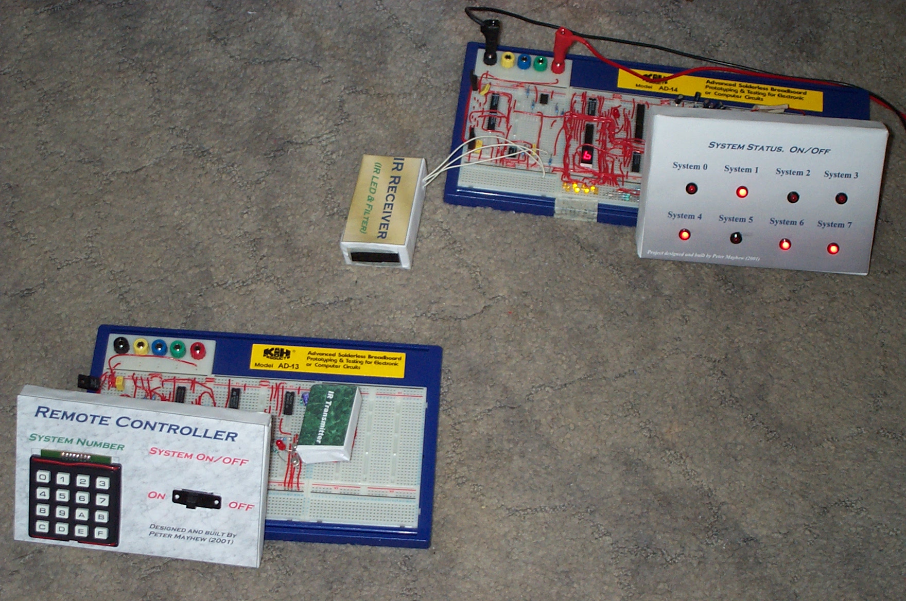
Initial Block Diagram
-
- To start the project a initial block diagram has been produced, which will most probably change/adapt as the project develops. This shows the general idea of how the project will be constructed, and will be used as the foundation to the project building.

Figure 1 Block diagram of system

Figure 2 Block diagram outlining basic principle of Project
Overview of system
-
- The project is based around any generic remote control which is used in everyday life.
- There will be a transmitter, which the operator will use and there is the receiver which will control the appliances.
- The project can control up to 8 appliances, switching them On or Off. This is done by presses two switches on the transmitter. Switch 1 control the ON OFF state, this is known as the STATUS, and switch two is actually a matrix keypad of 0 – 8, to control each appliance.
Brief overview of block diagram
-
-
- The idea behind the project is to gather the information from the user, which will be obtained from the switches, as shown in Figure 2. Once the user has pressed the STATUS switch to either On or Off, and has pressed one of the buttons on the Matrix keypad, the transmitter will store, modulate and transmit this information Infra Red LED to the receiver.
- The receiver will detect this Infra red light and demodulate the signal. Providing the data received is valid code, it will be stored in a register. The important information is then extracted from the could, such as which system to control, and whether is should be On or Off.
- The information is then used to control the appropriate system.
- This is a brief overview. The project will now go though a detailed explanation of
-
- Infra red light
- The Transmitter
- The Receiver.
-
- Since the transmitter and receiver has been designed using Logic IC’s the project has been split into many sections, so it becomes more manageable.
-
Theory behind Electromagnetic Radiation and IR
-
- To begin the project design, an insight is required into the theory into Electromagnetic Radiation and Infrared.
- Electromagnetic Radiation is a form of energy, where we can observe this as light. A definition of Electromagnetic radiation is: a kind of radiation including Visible Light, Radio Rays, Gamma Rays, X-Rays, and Infra-red Rays etc.
- A pictorial representation of Electromagnetic Radiation is shown in Figure 3. The electric field and magnetic field are always 90 degrees to each other. E is the electric field and is the magnetic field.
- This is also known as a transverse electromagnetic waveform. (TEM Wave)
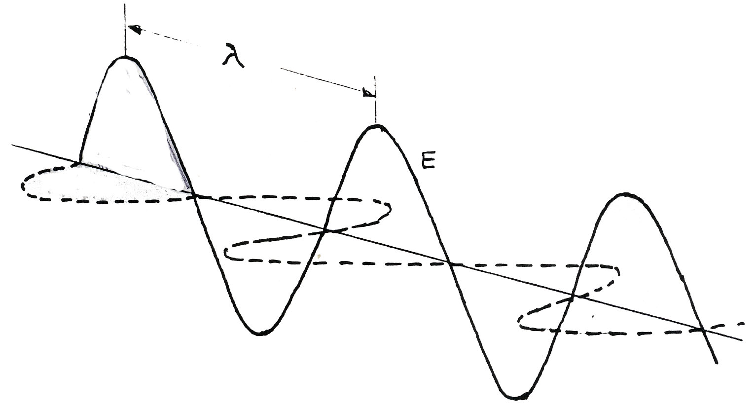
Figure 3 Pictorial representation of Electromagnetic Wave
-
- Light is a particular range of wavelengths which can be detected by the human eye. These wavelengths range from (approx) 10mm to 6m.
- Different types of electromagnetic radiation have different wavelengths or frequencies. From radio waves through visible light to gamma rays.
- It must be noted that all electromagnetic waves travel at the same velocity, which is approximately 300,000,000 Metres per second in a vacuum, hence the speed of light.
- The main difference between the electromagnetic radiation wavelengths is their interaction with matter
- The different wavelengths are shown in Figure 4.
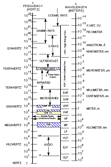
Figure 4 Electromagnetic Spectrum
-
- The waves travel in a straight line but can be affected by:
- Reflectance. Which is the reversal of direction that occurs at the surface of an object i.e. a mirror.
- Refraction. A change of the angle that occurs at the boundaries of different surfaces. Different wavelengths have different angles of refraction i.e. a stick apparently bending in the water.
- Diffraction. Which is a deflection that occurs at apertures or edges of objects.
- The two main materials used in producing Infra Red sensors are Silicon and Germanium. As shown by Figure 5 both have different spectral responses. Germanium has a high response at the upper wavelengths, where as Silicon has a high response at the lower end of the infra red spectrum
- The waves travel in a straight line but can be affected by:

Figure 5 Graph showing spectral response of Germanium and Silicon
-
- One advantage that infrared waves have is that they will often penetrate smoke, haze and fog better that visible light because the infrared waves are longer than the particles in the atmosphere that block visible light.
Inverse Square Law Of Illumination
-
-
- As the luminous flux travels away from the light source the area over which it spreads increases, therefore the illuminance (lux) must decrease. The relationship is expressed by the inverse square law and illustrated in Figure 6.
-
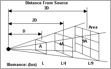
Figure 6 Inverse Square Law Of Illumination
-
-
- The relationship between illuminance and it’s effect at a distance is given by:
-
The Transmitter
-
- The transmitter is split into several sections, are there are many different parts, which build up to a complete transmitter.
Inputting data
-
-
- In order to obtain information on which system to control, the user will have to tell the controller.
- The can be done by having a keypad, where the used will physically tell the controller by using a keypad
- The keypad is quite straight forward. First, tell the controller whether it will activate or deactivate the system by pressing the “System On/Off” Switch. Then press one of the buttons from 0 to 7.
- So if the System On/Off switch is switched to the ON position and button 2 is pressed, this will store a code to Switch system 2 ON.
-
Figure 7 Keypad
Interfacing Keypad with the transmitter
-
-
- In order to interface the keypad with the transmitter a IC (Integrated Circuit) is required to convert the switch matrix into a digital code for the transmitter to use.
- If button TWO is pressed, the keypad will recognise it as Row 1 Column 2. This is shown in Figure 8.
-
| Co-ordinate | Logic level |
| Row 1 | 1 |
| Row 2 | 0 |
| Row 3 | 0 |
| Row 4 | 0 |
| Column 1 | 0 |
| Column 2 | 0 |
| Column 3 | 1 |
| Column 4 | 0 |
-
-
- Thus button number two is now represented by a six bit digital code.
- The keyboard can be represented as a schematic diagram.
-

Figure 9 Switch matrix
-
-
- The interfacing of the keypad to the controller can be done using a 74C922, which is a 16-keypad encoder.
- The 74C922 provides all the necessary logic to encode an array of switches.
- This particular IC can also reduces de-bounce which can cause erratic results. This will be mentioned in more detail later in the project.
- This IC can store up to 2 key roll over.
- A question may be asked why a 16 key encoder is used when there is only 8 buttons for the 8 systems to be controlled. The research so far has shown that there is only encoders for 16keys and 20 keys. Thus, the closest match is the 16 key encoder.
- The actual keypad that will be used is shown in Figure 10.
- The keypad is manufactured by a company called EAO Secme SA. Made in France. The keypad was chosen, as it is very ergonomic and simple to use and integrate into the circuit. The cost of the item was very attractive at £5.
-
Electrical Bouncing
-
-
- This is where a key is pressed and a mechanical contact is made, thus producing a closed circuit. Sometimes the contacts can take a few milliseconds to make a proper contact.
- Within this period the two contacts may produce several spikes where it makes and breaks the circuit as shown in Figure 11.
-
-
-
- These spikes can be misinterpreted as signals. The 74C922 does incorporate de-bouncing which will overcome this problem.
- Only a signal external capacitor is required in order for the IC to overcome this problem.
- The correct capacitor was found by looking at a graph on the data sheet on page 7.
- This graph is shown below in Figure 12.
-
Figure 12 Graph showing de-bounce capacitor required
-
-
- By looking at the graph a suitable de-bouncing period would be 100ms. This shows that a 10F (approx) is required. This is shown by the red line on Figure 12.
-
Enabling outputs
-
-
- The 74922 requires an additional component as it will not output any code until the has a logic 0 applied. This is because the outputs on the 74922 are Tristate NAND gates.
- It is called a Tristate as there are three possible conditioned. Logic 1, Logic 0 and High Impedance (Hi-Z). Hence the new condition is the Hi-Z. This is a condition where both transistors in the totem pole arrangement are turned off so that the output is at a high impedance in respect to ground and VCC.
- In order to allow the Tristate NAND gates to become enabled a logic 0 is required (remember that it is active low).
- When a key is pressed the data available goes high, this can be inverted and used to enable the outputs. This is shown below in Figure 13.
-
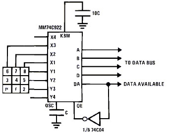
Figure 13 Example of enabling outputs
-
-
- A timing diagram is shown in Figure 14. This shows that once a key has been pressed (logic 0) and the bounce period expires the data available pin goes high, then after a period of tpd0 the data output goes low.
-

Figure 14 Switching timing diagram
-
-
- The 74922 also reduces the amount of bits required. There is 7 bits used to locate each key, but the 74922 reduces this to 4 bits. This is useful as there will only be 8 bits in total to use in our transmission. This will be mentioned in more detail later.
-
The Clock
-
-
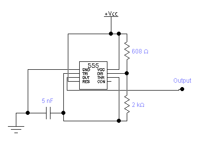
- The clock will be designed using a 555 timer, running at 17.8Khz.
- Using the 555 timer data sheet, the correct components can be determined by using the following formula.
- The formula is . Rearranging this formula for RA.
- If we have the capacitor is 10nF, and RB is 1.5K and knowing that the frequency of the cock will be 17.8KHz, this will mean that RA will need to be:
- A circuit was designed and simulated using Electronics Workbench, as shown below in Figure 15
-
-
-
- A oscilloscope was connected to the simulated 555 timer to show the periodic time, as shown in Figure 15.
-
Periodic Time

Figure 16 Periodic time for the 555 timer
-
-
- Since the periodic time is 55.6S, the frequency therefore must be
- The main concern is that the clock on the transmitter and the receiver has a frequency as close as possible other wise data could be lost. Since only 8bits of data is being transmitted, the timing of the project is LESS critical, see paragraph 12.11.11 on page 43, for more information.
- Practical tests on the 555 timer clocked showed that the frequency was running at 17.8KHz
-
Storing the information
-
-
- In order to store the information a register will be required. The information to be stored is as follows:
-
- Start bit 2 bit Fixed
- Information 4 bits Variable
- Stop bit 2 bits Fixed
-
- This accounts for the 8 bits in total which will be transferred
- To store this information an 8 bit register will be required. There are several IC to choose from two popular 8 bit registers are the :
-
- 74273 Octal D-Type Flip-Flops with Clear
- 74373 3-STATE Octal D-Type Latch
-
- The 74273 will be used in this project; there is no particular reason apart from being familiar with this IC through past project. Both IC are evenly matched.
- By using the 8 bit register, all the required information can be held for the for the system to use. Without this IC there would be critical timing difficulties.
- A schematic of part of the circuit is shown in Figure 17. Due to the components used the entire circuit cannot be simulated using Electronics Workbench. However, Figure 17 shows the 8-bit register connected to the 8 big shift register. The load switch shown will not be used in practice, as the data available pin on the keypad encodes will be used to clock the 8 bit register as previously mentioned, but this can not be simulated unfortunately.
-
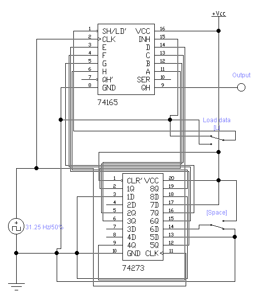
Figure 17 8 Bit register and 8 bit shift register
-
-
- When the user presses a button on the keypad, the keypad encoded input the 7 bit codes which defines which key is pressed by a matrix, and encode the data into a 4 bit This code is only on the output of the keypad encoder for a short period of time. The system would have to read and transmit the information before the keypad encoder discards the information and returns to it default logic 0 on the outputs.
- This problem could possibly be overcome by altering the keyboard scan, hence by altering the capacitor COSC. However, for reliability the 8 bit register will solve the timing difficulties.
- Once the information has been captured in the 8-bit register, it needs to be outputted serially. This can be done by using a 8-bit shift register.
- The 74165 would be the most useful as it can store the data and shift the information out so that it can be transmitted serially at a later stage. The partner to this IC can then be used in conjunction at the receiver, which will be the 74164, more information on this later.
- The 74165 loads the information at its ports directing into it internal register when the Shift/Load pin goes logic 0. When the Shift/Load pin goes to logic 1, the ports no longer read any more information, and the information in it internal register get shifter from ports QA to QH, in a serial manner.
- This is shown by a timing diagram in Figure 18.
- Ideally the data should be loaded and outputted automatically when a key is pressed, thus avoiding additional responses from the used to tell the system to load the data, as this would be inconvenient.
- This can be done automatically when a key is pressed by using the Data Available pin on the keypad encoder.
- When a key is pressed the Data Available pin goes logic 1, then logic 0 when the key is released. Thus, the keypad encoder Data Available pin can be used to directly control the shift/load pin on the 8-bit shift register. Thus, the 8-bit shift register now automatically loads and outputs data.
- As the data is outputted serially, it will be amplified ready for the IR LED.
-

Figure 18 Timing diagram for the 74165, 8 Bit shift register
The SSD
-
-
- Before transmitting the data the system should tell the user which button was pressed. Reassuring the user that the system is working correctly.
- The data being transmitted around the circuit can be used to drive a Seven Segment Display (SSD used henceforth). This will allow the user to see the system has recognised that the key has been pressed; basically it provides feedback to the user.
-
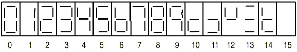
Figure 19 Characters that the 7447 can drive
-
-
- The SSD is basically seven LED’s arranged in a package. By passing current through a certain combination of LEDs the device can appear to display a number (or even a character if a different SSD driver is used). See Figure 20.
- Each connection from the decoder (7447) to the SSD required a current limiting resistor. This will prevent the LED from drawing too much current and overheating. The correct value of the current limiting resistor can be found by using the following formula:, thus .
- Since we have to use the closest available resister, a 270Ω was used.
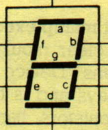 There is only one connection per segment as all of the anodes of the LEDs are connected together and taken to +Vcc The code which is sent from the SSD decoder will illuminate specific segments of the SSD to produce a character.
- Hence if you want the numerical value 4 to appear you would illuminate segments b, c, f, g.
-
Figure 20 Seven Segment Display
The SSD Decoders
-
-
- In order for the SSD to display the correct number, a SSD decoder is required. The SSD decoder will input the 4-bit binary code, which is created by the 74922 keypad encoder. These 4 bits will then be used to define which number to display on the SSD. Table 1 shows all the 4 bit binary codes and their associated characters.
- A 7447 will be used to perform this task. This IC will interface the circuit to the SSD. Without this the SSD decoder, the SSD will be unable to illuminate the correct segments and thus the correct character.
- These four bits will be sent to a 7447 IC on Inputs A – D. The IC will then encode the information, and output a code on “Outputs a – g”. This will be used to drive a SSD, to display the characters.
- Additional features of this IC allow a lamp test. If this pin is taken to a logic 0, then all the seven segment on the SSD will be lit, hence the term lamp test.
- The BI/RBO and RBI pins are used if you want to suppress zeros. Hence if you have four SSD’s, with 0, 0, 8, 2 respectively, being used a counter, you might want to suppress the first two zero’s. This is shown in Figure 21
- To blank leading zeros, the highest order pin should be connected to ground., then connect pin to pin of the next lowest order decoder, etc.
- Since 4-bit are used, there are a total of 16 different combinations, hence 14 different character can be displayed.
- The character that the 7447 can decode is shown below in Figure 19.
-
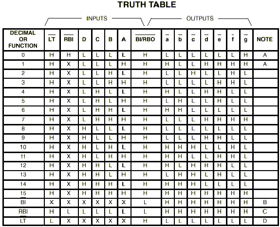
Table 1 Truth table for Seven Segment Display decoder

Cascading the Clock
-
-
- Originally the data transmitted was going to be modulated, but this became unpractical at a later stage in the project due to the time required to research and develop.
- However for the purpose of the project write up, the section has been kept.
- The clock was going to be running at 62.5Khz using a 555 timer.
- Since the main clock is a 555 timer running at 62.5Khz, this could be used for the carrier signal. In order to modulate the data, the data needs to be running at a much lower frequency.
- A separate clock could be used to provides a slower signal. An alternative option is to slow down the clock. This can be done by using a series of JK multi-vibrators.
- The JK Bistable multi-vibrator is also known as a flip-flop.
-
| J | K | CLK | Q |
| 0 | 0 | PGT | Q0 (no change) |
| 1 | 0 | PGT | 1 |
| 0 | 1 | PGT | 0 |
| 1 | 1 | PGT | Q0 (toggles) |
PGT = Positive going transition
Table 2 JK flip-flop logic table

Figure 22 Positive edge triggering JK flip-flop
-
-
- A JK flip-flop has a special condition when both J & K are set to logic 1. The output toggles on each positive edge of the clock.
- The two flip-flops are connected via Q1 and CLK2. A diagram demonstrates this in Figure 23. All the following is taken to a logic1 for the IC to produce a binary output. K1, K2, J1, J2, CLR1 & CLR2.
-

Figure 23 JK Flip-Flops connected together
-
-
- An input signal will be applied to the first flip-flop. This is a known as the Clock signal. In this case it will be the 62.5KHz signal from the 555 timer.
- The input of the JK will be 62.5KHz. This bistable signal on the input of the 1st flip flop will cause a bistable signal on the output of the flip-flop. But the signal on the output will be exactly ½ the clock frequency to 32.25Khz.
- A second JK flip flop will once again reduce the clock by halve, this will mean that the signal will now run at 15.63KHz.
- However since removing the idea of modulating the data, the clock frequency has been reduced, down to 17.8Khz, for no reason apart from component availability for the 555 at the time of construction.
- The overall clock frequency will therefore be halved. This is shown in Table 3 & Figure 24.
-
| Stage | Frequency | Divide by |
| Input signal | 17.8KHz | 1:1 |
| 1st flip flop A | 8.9KHz | 2:1 |
| 2nd flip flop B | 4.45KHz | 4:1 |
| 3rd flip flop C | 2.225KHz | 8:1 |
| 4th flip flop D | 1.1125KHz | 16:1 |
-
-
- NOTE, the actual clock frequency is now 1.1125Khz.
-

Figure 24 JK Flip-Flop Waveform
-
-
- The schematic the circuit used is shown in Figure 25. The IC used was a TTL 7476. Which is a dual JK Flip-Flop.
- Each IC contains 2 flip-flops; this will mean that two 7473’s will be required to output the correct frequency.
- Each IC consists of:
-
- 2 clock inputs
- 2 J inputs
- 2 K inputs
- 2 Clears
- 2 outputs
- 2 Complemented outputs.
- Positive and negative rail.
-
- The first JK clock input, is where the original signal will be inputted. This will be taken directly from the 17.8Khz 555 timer. Both the J & K will be taken to logic 1 in order for the flip flop to toggle. The clear pin will also be taken to a logic 1 so that the device is not clears (there is no requirement to).
- The output “Q” will then be used as the input for the second JK flip flop. Each additional flip-flop will be cascaded into the previous one, thus producing a lower clock frequency.
-
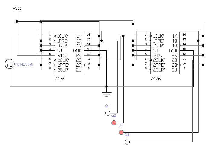
Figure 25 Schematic of JK Flip-Flop circuit
Enabling the IR LED
-
-
- When using the IR LED it was noticed that Infra Red light was being generated continuously this was because the IR LED was being fed a constant 5V. This was due to the 74LS165 producing a logic High (5V) while idle.
- To prevent this from happening a one shot was used in combination with a LOGIC AND gate.
- One input of the AND gate would be connected to the output of the 74LS165 (hence the data), and the other input to the AND gate would be connected to the output of the monostable.
- The monostable will be triggered by on the 74922, which will go HIGH on a key press.
- Under idle conditions, hence when no button has been pressed, the monostable will produce a constant Logic 0. This will cause the AND gate to produce a Logic 0 on the output no matter what the 74LS165 is sending, hence the data is blocked/disabled from the IR LEDS.
- Once a button has been pressed the 74922 will produce a Logic 1, which will inturn trigger the monostable to produce as Logic 1 for a predetermined period. This will allow the data from the 74LS165 to pass through the AND gate, hence the output have been enabled.
- After a brief period has elapsed the monostable will revert back to a logic 0, and prevent anything else passing though the AND gate until another button on the keypad is pressed.
- This was designed using the following circuit configuration, as shown in Figure 26. (Note: Electronics Workbench does not support the 74LS121 so a Monosable is used in the diagram below for example purposed only)
-

Figure 26 IR LED enable circuit
-
-
- The formula for calculating the pulse width for the one shot is :
-
- Where RX is in Kilo Ohms
- CX is in Pico Farads
- TW is in nano seconds
- K = 0.7
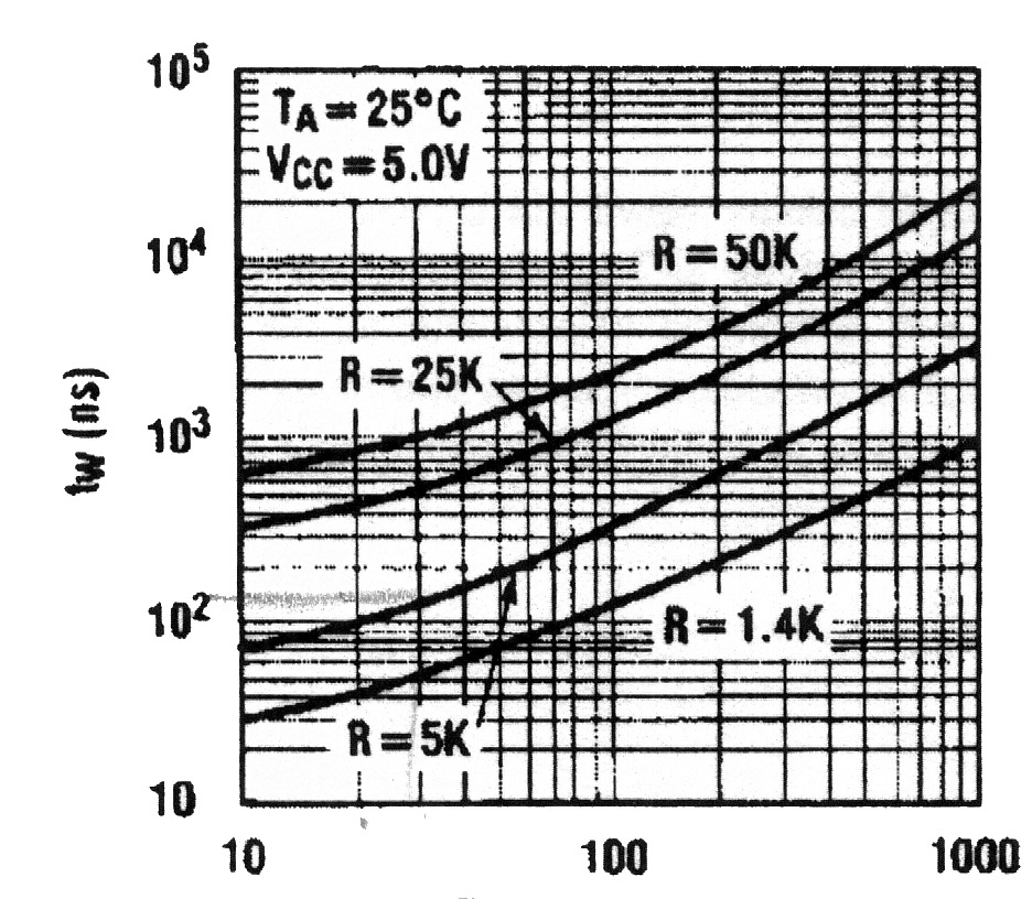
Figure 27 Graph showing characteristics between the pulse with, capacitance and the resistance
-
-
- The pulse needs to have a logic 1 to cover the duration when the data is outputted serially. The data to be transmitted has a duration of 15.6mS.
-
Remember, that the time is in Nano seconds, which means
This pulse width if perfectly sufficient
Infra red noise
-
-
- The data transmitted will be in binary, hence a DC voltage at either 0 Volts for Logic 0, or 5V for Logic 1.
- If the data was transmitted using these DC values, the IR LED would simply switch on and off with each logic signal.
- At close range, and with no interference, this method would work. But at distance, the signal will pick up stray infrared signal, coming from objects such as fluorescent lamps.
- This stray infrared noise can superimposed themselves on the data transmitted and hence corrupt the data. If the data becomes corrupt and cannot be repaired, then the receiving system will be unable to extract the correct information from the signal, and hence the system will function erratically or not at all.
- In order to overcome this problem, the data transmitted need to be immune to stray infrared signals.
- One method is to use a filter.
-
Filtering out IR noise
-
-
- By using a filter, any unwanted light outside a set range will be attenuated so they cannot pass propagate any further beyond the filter.
- The wavelength that will be used by the IR emitter and receiver will be 950nm. Thus we need to allow this particular wavelength to pass through the filter but block any other wavelengths.
- A company called Peerless Plastics and Coasting produce a plastic with a special coating. This coating acts as a filter.
- The spectrum response for the filter is shown in Figure 28. It shows that will allow wavelengths above 750nm to pass through with >90% transmission. Any wavelengths below 750nm will be greatly attenuated. Wavelengths <660nm will be completely blocked.
-
System operates at this wavelength
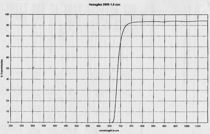
Figure 28 Spectral response for filter
-
-
- A disadvantage of using this filter is that even the wanted wavelength will be attenuated slightly the highlighted wavelength, shown in Figure 28 shows that the maximum transmission percentage is approx 95%.
- This means that 5% of the require signal strength will be lost. In order to overcome this, the signal will have to be amplifier.
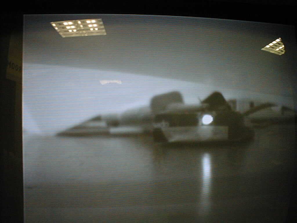
- Figure 29 shows a picture taken of one of the IR LED used in this project. This was taken using a Black/White CCD camera. The image clearly shows the infra red light, which could not have been seen without the camera. The infrared light is shown as a bright white dot.
- By looking at the image, not only can the infrared light be seen, but also other object surrounding it, due the ambient light also captured by the camera.
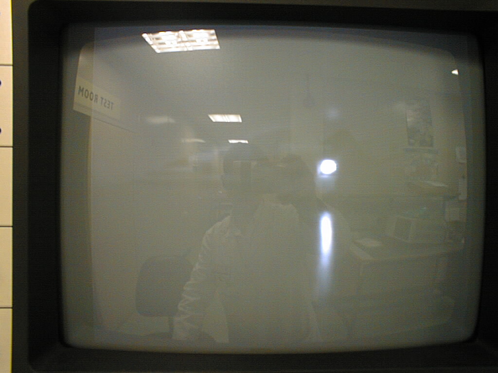
- Since there is natural Infrared light surrounding us in everyday life, a filter will be required to remove this.
- By using an IR filter, all none appropriate wavelengths can be blocked, thus allowing the system to just sense detecting IR and not ambient light.
- By placing this filtering in front of the CCD. Hence all of the ambient light should be blocked and IR light should pass through the filter. A second picture was taken with the filter in front of the CCD camera, this picture is shown in Figure 30.
- Clearly all-ambient light has been removed, and the IR from the LED is very clear. Objects in the picture can be seen, but this is the reflection off the monitor used to display the images from the CCD camera.
-
-
-
- Using this filter does reduce the signal/noise ratio, but between the transmitter and the receivers filter, stray electromagnetic waves can still become superimposed onto the transmitted signal.
- In order to solve this, the transmitted signal needs to be immune to the noise surrounding it. This can be done by modulating the signal.
-
Amplifying the signal before transmission
-
-
- Now the data is ready for transmission, it needs to be amplified, as the IC cannot source enough current to power the IR LEDs sufficiently. To rectify this a basic transistor amplifier will be used for each IR LED.
- The circuit works by inputting the data to the “data pin” as shown in Figure 31. The binary pulses will then be sent through the two resistors. This is so the transistors are not overdriven.
- With each DC pulse the transistors will switch on, and provide a 5V supply with only 33 resistance. This will mean that 152mA will flow through the IR LEDs, which will illuminate them both very brightly.
- This is important, as the brighter the IR LEDS are, the further the light will travel. As mentioned earlier in paragraph 8.13 on page 12, due to the inverse square law, the light will become more diffused as the distance increases.
- Although this is a lot of current to pass through the IR LEDS, the pulses are very short. Each one in fact is , , . This is very a very short period of time, as the IR LED should not overheat and become damaged.
-

Figure 31 Transmitter amplifier
Infra red light
-
- In order to carry the information from the transmitter to the receiver, infra red light will be transmitted.
- This will be done by sending the information through an Infra Red LED.
- Unlike ordinary LED’S, IR LEDs will not illuminate to the naked eye. This is because IR is out of the human eye spectrum.
- The are several issues with the IR LEDs which have to be address.
IR Output mW
-
-
- All the emitters will require current to give an output of power. All emitters however require different amount of current to produce X amount of mW output. A couple of emitters have been taken from Farnell Catalogue to illustrate this in Figure 32.
-
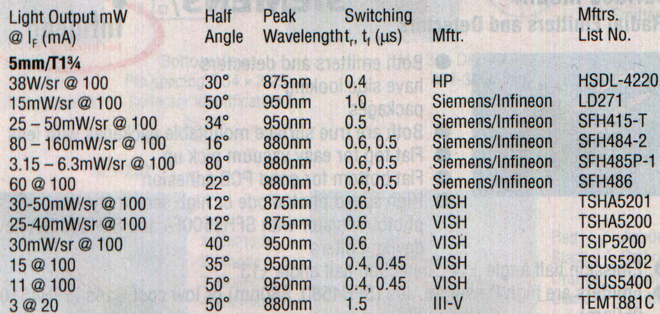
Figure 32 Example of Emitters characteristics
-
- First look at the 1st column, LIGHT OUTPUT (I do not personally agree with this term “Light output” as used in the catalogue as no light in the visible spectrum 390 –740mm is produced). There is two important factors here in Figure 32. The IR Output (mW) and the IF (mA). Clearly we want the most output power per mA, hence efficiency.. Looking at Figure 32, the most efficient emitters are the SFH484-2, SFH415-T and TSHA5201.
- These three emitter have good efficiency, particularly the SFH484-2
Wavelength IR LED operates at
-
-
- It is very important that the emitter and detector operate on the same wavelength, otherwise the detector will not receive maximum power. A wavelength of approximately 950nm is required, due to the type of detector used later. This means that the LD271, SFH415-T, TSIP5200,TSUS5202, TSUS5400.
- These have a maximum peak response of 950nm, which will give maximum power transfer to the detector.
-
Angles which the IR LED transmits.
-
-
- It is preferable for the emitter to have a small angle. This way the signal is more concentrated. Otherwise the power transmitted will reduce rapidly due to the inverse square law. The emitters with a small angle is HSDL-4220, SFH484-2, SFH486, TSHA5201, TSHA5200.
-
Conclusion on Emitters.
-
-
- Three of the emitters in the list appear to suitable in two out of the three requirements, these emitters where the TSHA5201, TSIP5200, SFH415-T.
- Since the SFH415-T had the best match wavelength and higher IR output, this IR LED was chosen. (This LED is now called a SFH415-U in the new Farnell catalogue).
- An image of the IR LED used is shown in Figure 33.
-
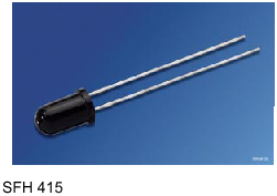
Figure 33 Picture of a SFH415U Infrared emitter 5mm
Maximum current IR LED can handle
-
-
- As more current is passed through the LED it will radiate more IR. The problem is the emitter will get warm as it tries to dissipate the power (P=I*R),
-

-
-
- Since a heat sink is not a feasible option, another method is to pulse the current to the emitter.
- Buy pulsing, the emitter will have a time period where current will be drawn and the emitter will heat up, then there will be a time period where there will be no current drawn and the emitter will cool down. The capability of pulsing the SFH415-U, is shown in Figure 34.
- The more current that is passed through the IR LED, the greater the intensity of the radiation.
- It is in great interest that the infrared emitter is transmitting optimally. If the signal transmitted by the emitter is too weak, everything beyond this stage will be progressively worse.
- This is because as the signal propagates the area it covers increases. This is all covered by the inverse square law.
-
Figure 34 Characteristics of pulsing the emitter
Noise immunity
-
- In order to prevent the signal from being susceptible to the Infra Red noise apparent, this signals needs to be immune. Possible methods are shown below:
- AM (Amplitude Modulation)
- FM (Frequency Modulation)
- PM (Phase Modulation)
- Parity Checks
- Sending signal more than once.
- RC5
- RECS 80
- Other methods of modulation are available such as Phase modulation and Pulse Code modulation. But this is beyond the scope of this project.
Amplitude Modulation
-
-
- Amplitude Modulation is varying the amplitude of a carrier in symphony with the base band
- The Base band is the information, which we want to transmit, in this case a series of DC logic pulses.
- The Carrier is a high frequency oscillation, i.e. 1Mhz clock. The carrier amplitude will be dependent on the amplitude of the base band.
- The data to be transmitted will be eight bits. The eight bits are DC pulses of 1V and 0V.
- An example of this is shown in Figure 35.
-
Amplitude Modulation
DC signal
(Baseband)
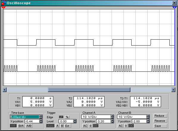
Figure 35 Amplitude modulated DC signals
-
-
- If the data is modulating by AM, the receiver needs to be able to detect the information and remove the noise.
- If the carrier signal was set to 1Mhz, the receiver could be set up to only allows signals oscillating at 1Mhz, thus blocking any unwanted signals, especially fluorescent lamps which will flicker at 100Hz.
-
Advantages
-
-
-
- By using Amplitude Modulation, the signal is easy to modulate and demodulate.
- Although AM is susceptible to noise, the data transmitted consists of 1’s and 0’s, and thus the data can still be retrieved, and the noise can be removed using filters.
-
-
Disadvantages
Frequency Modulation
-
-
- An alternative to AM is FM, Frequency Modulation.
- FM is similar to AM, but the data is contained within the frequency of the signal, not the amplitude.
- This means that FM has far superior noise immunity is comparison to AM. An example of this is shown in Figure 36.
-
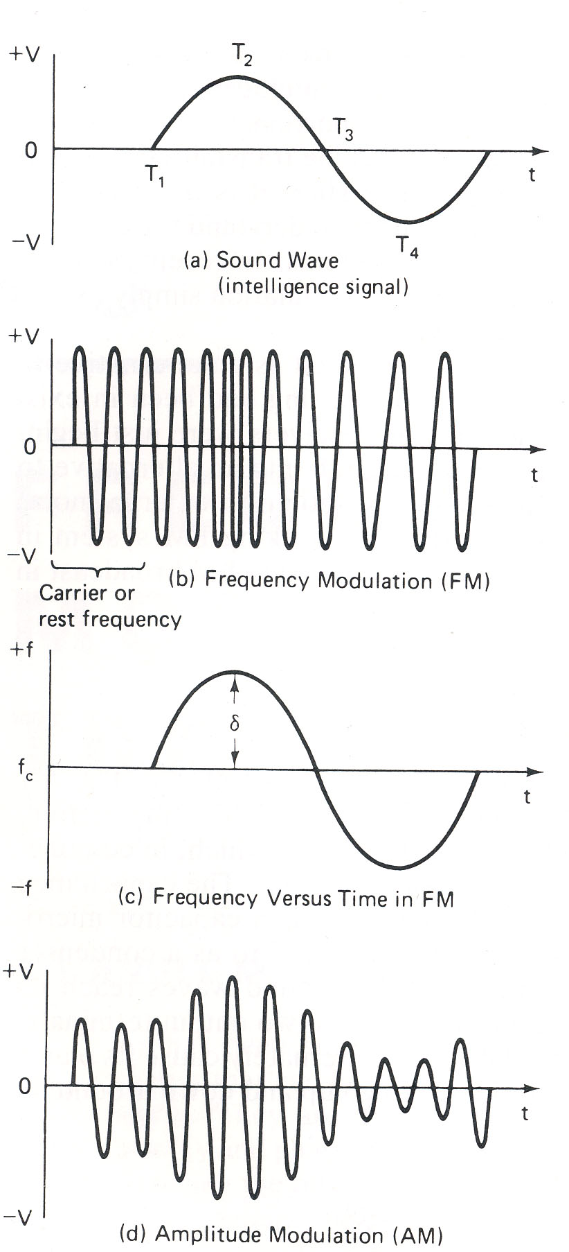
Figure 36 Example of Amplitude and Frequency Modulation
-
-
- Even though noise can still be superimposed upon, when the signal is demodulated, hence the data contained is extracted. The noise present will have no effect on the actual signal.
-
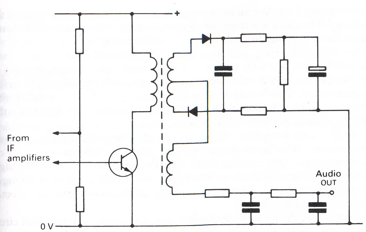
Figure 37 FM receiver using discrete components
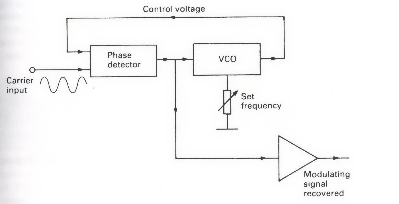
Figure 38 FM receiver using a Phase Locked Loop (system diagram)
Advantages
-
-
-
- The signals are immune to noise
-
-
Disadvantages
-
-
-
- The circuit required to modulate the signals are demodulate the signals are more complicated.
-
-
Adding parity checks to the signal
-
-
- Currently the data send consists of:
-
- 2 start bits
- 5 data bits
- 2 stop bit.
Sending the signal more that once.
-
-
- By sending the signal twice, the receiver could compare both transmissions, if they are the same then the signals can be assumed to be correct.
- If the signals are different, then the signals can rejected, as being corrupt.
-
Advantages
-
-
-
- The data from both transmissions can be compared, and if they are different, they can be rejected, and the used can be alerted this to the problem, by illuminating a LED.
-
-
Disadvantages
-
-
-
- This method is unnecessary complicated, and the data will be rejected if both transmissions are different.
- Better results can be achieved by modulating the signal
-
-
RECS 80
-
-
- RECS 80 a common IR transmission standard for remote controls. PCM stands for Pulse Length Modulation . (PLM)
- PLM works by varying the length of the bits by a specified duration of “T” in accordance with the bit logic. Hence a logic 1 is a high level followed by a duration of T. Logic 0 is a high level followed by a duration 2T. The diagram below demonstrates this.
-
Figure 39 Example of RECS 80 code
Disadvantages
-
-
-
- The disadvantage of PLM is that a logic 1 takes longer to transmit in comparison to a logic 0.
-
-
RC5
-
-
- RC5 is the alternative IR transmission standard that many manufactures use. The main difference is the code has a constant duration for all the bits transmitted. But the bits are encoded in the following manner. A logic 0 is a HIGH followed by a LOW. A logic 1 is a LOW followed by a HIGH. This is also known as “BI-PHASE”.
- This method is produces a signal where all the bits have the same duration
- The disadvantage of this method is additional bits are required at the start of the data, and additional circuitry is required to encode the serial data.
-
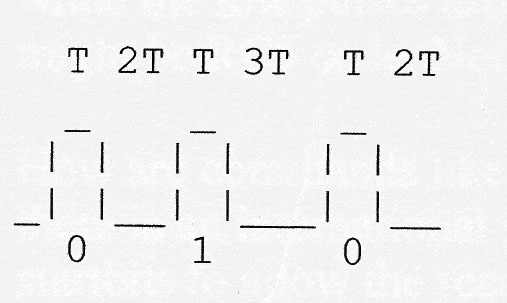
Figure 40 Example of RC5 code
Summery on noise immunity
-
-
- Although the data can be encoded by RECS 80 or RC5 etc, the data transmitted is still very susceptible to IR noise. The most common IR radiation comes from fluorescent lamps. This types of IR radiation appears at 100Hz pulse trains on the receiver, this is because the fluorescent lamp is switching ON and OFF 100 times per second.
- To overcome this problem the data is modulated. The most common form of modulation is Amplitude Modulation for the following reason.
- By modulating the amplitude of the signal, at i.e. 32KHz, this can be used for the receiver to TUNE into.
- Hence the receiver could be designed so that only signals with a frequency of 32Khz will pass through the first stages of the receiver and any other IR at different frequencies will be blocked.
- This method should allow the receiver to remove any unwanted IR noise within reason.
-
Preparing signal for transmission
-
-
- This signal now needs to be converted so that it can drive the IR LED. The LED needs a voltage of 1.25V. In order to have a amplitude of 1.2V and a current of 100mA.
- This way the illumination should be bright enough to radiate from the transmitter to the receiver.
- Since the LEDs will be pulsing very quickly this high current flow will not damage the IR LED’s, as there will be small periods in between the pulses where the IR LED can cool down.
-
Block diagram for transmitter
-
-
- The overall circuit is shown as a block diagram in Figure 41.
- This gives a general idea of how the transmitter fits together.
- Since modulation/encoding was not actually used in the practical project, it is not shown in the block diagram.
-
Figure 41 Block diagram for transmitter circuit
The Receiver
-
- In order to receive the signals an infrared sensor/detector is required. It is very important that the correct detector is chosen otherwise complications can arise when receiving the signals. Both the transmitter and detector will operate over a band width, but there both have a peak response i.e. peak infrared wavelength in which they are designed to operate at, see Figure 43. Ideally both the transmitter and detector need to operate on the same wavelength, otherwise the detector will not receive the full power of the signals transmitted
- There are two types of detectors, which will now be investigated.
A Phototransistor.
-
-
- This is basically a transistor where the base is controlled by the amount of infrared light it receives. Hence, as the IR light increase, the current across the collector and emitter increases.
- Figure 42 shows a list of detectors to use in the project.
-
IR Sensitivity mW
-
-
- All the detectors vary in how sensitive they are to infrared radiation.
- The most sensitive sensors in Figure 42 is the SFH313-2, SFH300-3, BPV11.
-

Figure 42 Example of Detectors characteristics
Wavelength detector operates at
-
-
- A detector which a peak spectral response of 950nm would be ideal.
- The detectors which have the best peak spectral response for this application is the BVP11.
-
Angles which the detector transmits
-
-
- It is preferable to have a detector with a wide angle so that it can receive signals from the transmitter from a wide range, the disadvantage of this is, it will pick up more stray infrared signals hence noise, making a worse signal/noise ratio. For this reason a narrow angle is required.
- The detectors with a narrow operating angle is the SFH313-2 and the BVP11.
-
Conclusion on phototransistor detectors
-
-
- The BVP11 stand out to be the most suitable detects as it has the correct peak response, a narrow operating angle and good sensitivity. This phototransistor is made by Vishay Telefunken.
- NOTE: After reading the data sheet it was found that the spectral peak response of the is 850nm not 950nm. This means that the detector will only receive a maximum of 70% of the transmitted power. This is shown in Figure 43
-
Peak wavelength
850nm

Figure 43 Relative Spectral Sensitivity vs. Wavelength
Alternative detectors
-
-
- An alternative to the phototransistor is A Infra red receiver module.
- This includes a Sensor to pick up the infrared light. A amplifier to increase the amplitude of the small signals received. A filter to remove any stray/unwanted signals, and a demodulator the 37.9KHz signal.
- This can significantly reduces the amount of components required on the receiver as most of the work is done by this IC.
- The possible IC to be used is the PIC12043SM made by Kodenshi.
- This particular IC has improved electromagnetic interference resistance, which means that it will be more reliable in picking up the correct signals.
-
Amplifying the received signal
-
-
- When the signal is received, the amplitude will be small, and hence it will need to be amplified in order to be of any use. To amplify the signal a transistor, FET or Op-amp could be used.
- Using a Op-amp would be beneficial since was more appropriate for the following reasons:
-
- Higher gain
- Better reliability
- Better stability
Offset compensation
-
-
- A schematic of the circuit is shown in Figure 44.
-

Explanation of power amplifier
-
-
- The circuit (Figure 44) was then constructed, and it worked successfully.
- Pin 6 was linked to ground; this means that the output will be dependent on the signal present on the none-inverting input (pin 2)
- This is because the output is proportional to the differential of the two inputs.
- To control the input signal amplitude a potential divider (POT) is used.
- The input signal is connected such that the signal will pass through the POT.
- If the POT is set the its minimum resistance, the full signal to be connected to the LM380 +Ve input (Pin 2)
- If the POT is set to its maximum resistance value, the signal will be attenuated and thus only a very small proportion of the signal will be reaching the reaching the +Ve input.
- C1 is used to remove any low frequency noise coming from the power supply, such as mains 50Hz hum superimposed upon the DC voltage. (This can arise due to a poor smoothing design in the power supply).
- C2 is the bypass capacitor, and is connected to bypass pin (pin 1). The purpose of the bypass capacitor is to allow the input signal to flow through, and prevent the signal from altering the gain of the circuit. Without this capacitor, the potential difference across the internal circuitry will very in accordance with the signal, and thus cause the biasing to alter, and change the gain of the circuit.
- Pin 8 is the output of the amplifier, and should be connected to the load, which is the 8 3W resistor in this experiment.
- Pins 3, 4, 5, 7, 10, 11, 12 are connected directly to ground.
- Pin 14 is connected directly to the positive supply.
-
Synchronisation
-
-
- Without synchronisation between the transmitter and the receiver, the will both fail to communicate. The two methods of communication are Synchronous and Asynchronous.
-
Synchronous
-
-
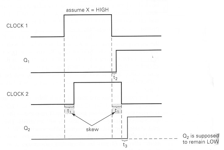
- By using synchronous communication, there will be a single line of communication to transfer the serial information, and a separate connection for the clock. Thus the clock on the transmitter will be the same as the clock on the receiver this is a disadvantage, as more connections are required. The advantage is that no data will be lost due to phase differences between the clock on the transmitter and the receiver.
- It must be noticed that the clock connected between the transmitter and the receiver must be minimal for high speed systems as a timing problem such as CLOCK SKEW can occur.
- Clock skew is where the propagation delay between the clock travelling from the transmitter to the receiver is such that there is a slight phase shift between the clock on the transmitter and the receiver. This is shown in Figure 45.
-
Asynchronous
-
-
- Asynchronous communication has the advantage where less connections in which to communicate, as in this case, only the data will be transmitted, no separate clock signals.
- In this project only one stream of data can be transmitted, hence the data, it will not be possible to send a separate clock as well, without making the project much more involved.
- If a separate clock signal was transmitted along with the data, Time Division Multiplexing would be required, and would make the project much more complicated and out of scope.
- By sending the data asynchronous the clocks on the transmitter and the receiver will be independent of each other.. The disadvantage is that the there the clocks could be out of phase and potentially cause information to be lost during transmission.
- If however a long string of bytes were to be transmitted, timing would be more critical, as the diagrams in Figure 46 & Figure 47.
- Figure 46 show two clocks, one on the receiver, and one of the transmitter. Both of the clocks are slightly out of phase. It can be seen the phase shift at the end of the transmitted by is slightly greater, but both clock do have a period where they ARE still in phase as shown by the blue crosshatch box.
-
Transmitter
Receiver
Phase shift
Phase shift
In phase

Figure 46 Sending one byte out of phase
-
-
- However, if more than one byte was transmitted, the phase shift between the transmitter and the receiver would cause problems, as shown in Figure 47.
- Toward the end of the transmission, the phase shift has caused the clocks to become 180 out of phase. This would cause serious timing problems.
-
Transmitter
Receiver
Phase shift
Phase shift180

Figure 47 Sending over one byte out of phase
-
-
- Since only 8 bits are being transmitted in this project, there should be no timing difficulties.
- However, if there are timing problems this can be overcome by encoding the data transmitted using i.e. Manchester encoding otherwise known as RC5 in the commercial trade
-
Demodulation
-
-
- This is the part of the circuitry, which will revert the modulated signal back to its original form.
- The section of the project will not be designed or constructed due to time restrictions.
- The demodulation processor must be the same as the modulation process. Hence is AM modulation was used on the transmitter, the receiver must use AM demodulator.
- Research has shown than AM is the simplest form of modulation. Assuming the data was modulated using AM on the transmitter, the following circuit will show how the signal can be reverted back to it original form.
- This circuit will assume the original signal was a sine wave.
-
The Envelope detector
-
-
- To demodulate AM, an Envelope detected is required. This will extract the information (base band) from the RF (Radio Frequency) AM signal.
- The first part of the envelope detector is a ½ wave rectifier, as shown in Figure 48.
-
-
-
- With the aid of a capacitor in parallel with the resistor, the output ripple can be reduce to a (almost) sine wave. Which was the original signal transmitted. The values of the resistor and capacitor have to be chosen with care, as the performance the this part of the circuit can vary drastically, with the CR time (time constant), and hence alter the output signal.
-
Figure 49 ½ wave rectifier with capacitor
-
-
- The next stage consists of a RC (resistive capacitive) filter, which reduces the RF ripple.
- At the end of the RC filter there is a DC blocking capacitor, which removes any DC voltage which offsets the signal, as shown in Figure 50.
-
Input Output
-
-
- The whole circuit is now shown in Figure 51.
-
Figure 51 Diode envelope detector
-
-
- Research has also been made into IR receivers currently being used in commercial appliances. A scrap IR receiver was removed from a video recorder and is shown in Figure 52.
-
IR Receiver from video recorder

Figure 52 Example IR receiver from scrap video recorder
-
-
- The protective cover was removed to reveal the inner electronics, as shown in Figure 53.
- The receiver is very compact, the picture shows the IR receiver, a IC which is most probably programmed, and a component labelled LR.
- I would guess this LR component is used to TUNE into the modulated IR signal being transmitted such that the receiver can remove any unwanted noise.
- The programmable IC will extract the information, and other capacitors could be used to decoupling and removing any high frequency received.
-
IR receiver
Programmable IC
LR Tuner
Decoupling and filter capacitors

Figure 53 IR receiver from scrap video recorder with off
System Controller
-
-
- The controller needs to first know which system will be controlled. To perform this function a System Controller will be used.
- The system controller circuit needs to be able to identify which system needs to be switched ON or OFF.
- There is only four bits of the data transmitted that is actually required. There are three bits, which contain the ADDRESS, and one bit which contains the STATUS.
- The address identity, states which system is about to be controlled. The addresses are shown in Table 4.
-
| Address code | System |
| 000 | System 0 |
| 001 | System 1 |
| 010 | System 2 |
| 011 | System 3 |
| 100 | System 4 |
| 101 | System 5 |
| 110 | System 6 |
| 111 | System 7 |
-
-
- If for example we have an address of 100 and a status of 1. This will means, switch ON SYSTEM 4.
- The first step is to get the address code. There are three bits used to assign the address. By using a de-multiplexer, 8 lines can be produced, in which to control the 8 systems. This can be done using a standard 74138 1-8 De-multiplexer.
-
De-multiplexer
-
-
- A multiplexer takes several inputs and connects one of these to the output to transfer the information. A de-multiplexer does the opposite. It takes one inputs and connects it to one of several outputs. A diagram of a example de-multiplexer is shown in Figure 54.
-

-
-
- The de-multiplexer works by receiving 3 bits, (this will be the address data received). These 3 bits will determines which output the de-multiplexer should selected. The truth table in Table 5 shows the operation of the de-multiplexer.
- A, B, C will be the 3 bits received. This was originally the BCD codes generated by the keypad encoder, see paragraph 9.3.5 on page 14.
- G1 will be connected to the Clock Pulse pin on the DN74LS273 (8 bit register).
- Each time the 8-bit register receives new date, the Clock pulse pin (pin 6) which produces a clock pulse.
- This clock pulse will therefore enable the de-multiplexer and allow it to read the new data.
- Under normal conditions, pin 6 on the 8-bit register will be active low, and hence this will inhibit the de-multiplexer from reading any more data.
- G2 is actually G2a and G2b. Both of these are active low and are not required for this circuit. Thus, they are both connected to ground.
- In order for the de-multiplexer to function, it needs a LOGIC 1 on pin 4, 5 and a LOGIC 1 on pin 6.
- Now one of the outputs is selected on the de-multiplexer the receiver knows which system to control. However, the de-multiplexer produces a logic 0 for the selected output, and this needs to be a logic 1 so it remains compatible with the rest of the circuitry.
- To accomplish this, an inverter (7404) will be connected between each output of the de-multiplexer.
- All 8 outputs are then connected to the next part of the circuit. The JK flip-flops. The address bits from the de-multiplexer will be used to clock the JK’s.
-

Table 5 Truth table for De-multiplexer
Status Bit & System Controller Registers
-
-
- Next, the controller needs to know whether the system should be switched ON or OFF. This data comes from the STATUS bit.
- The STATUS bit connected and stored directly into each JK flip flop. There are four flip-flops and two flips-flops in each IC, thus there are eight flip-flops in total, one for each system.
- Once a button is pressed, the status bit is sent to each flop-flop, to be stored.
- Since only one flip-flops will be selected by the de-multiplexer, only one flip-flop will be clocked, and hence store the status bit.
- The schematic for this circuit is shown below in Figure 55.
-
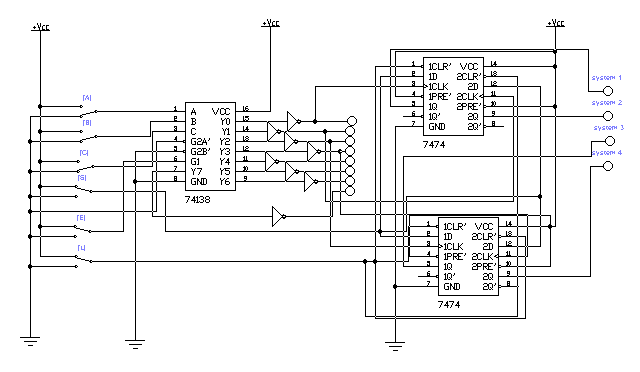
Figure 55 Control system schematic
Clearing The Registers During “Switch On”
-
-
- When the receiver is switch on, the flip-flops will contain invalid information. This will cause the system controller to switch “On” some of the systems during “switch on”. This is obviously a problem, and can be solved by resetting the flips flops during switch on.
- To over come this, the Clear pin on each flip-flop will be taken to logic 0 momentarily then back to logic 1 when the system is switch on. Thus, this will clear the outputs, and allow the controller to function correctly.
- To provide this momentarily logic 0, a one-shot mono-stable will be used. In this case, a 74121.
- This mono-stable will be set up to provide to small pulse and is calculated and designed using the same process as the monostable, the IR LED enable circuit in the transmitter on paragraph 9.11 on page 25.
- Problems were experience with this circuit as the controller would act erratically when switching the systems states On or Off. This is mentioned in more detail in the practical write up on paragraph 13.69 on page 61.
- This was possibly caused by oscillations/noise in the power lines going to the IC and into the signal. A 1F capacitor was connected from each output of the 74138 with respect to ground and this cured the fault. The reliability of the circuit has been greatly improved. This is new circuit is shown in Figure 56.
-

Figure 56 Improved control system schematic
The driver
-
- The final part of the receiver circuit is to drive each system. Already the receiver has the extracted the information and knows which system to switch ON or OFF. The next stage is to drive the system.
- The JKs, which have the underpinning whether the system should be switched on or off, cannot drive the system, as they cannot source enough current. In order to overcome this problem, the JK’s will be used to switch a bipolar transistor as then require very little current.
- The transistor could then be used in a common emitter configuration to drive a relay to control the system hence switch ON of OFF. This is shown in Figure 73. The box with the text “Control” which is basically the control circuit shown previously in Figure 56, all placed into one sub circuit to simplify the design.
- The output from the JK will switch on a transistor, which will drive a relay. The relays will be capable of driving most common equipment. Thus, the systems connected (Fan, light) can be changed without altering the circuitry, providing the voltage and current drawn by the system is within tolerance of the relay.
Figure 57 Schematic of the driver
Block Diagram for the receiver
Figure 58 Block diagram of receiver
Practical write up
-
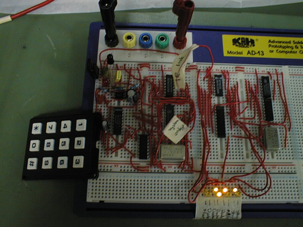
- The first build of the system was made on a Breadboard. This will allow the circuit to be built quickly, and altered if necessary with ease.
- To start off a 5v regulator using a 7805, 555 timer clock running at 4Hz was built and worked first time without any difficulties. The clock will run for this part of the test period at 4Hz show the transmission of data can be monitored using LED and a scope. This clock frequency will be increase at a later stage in development.
- After integrating the keypad encoder, so that the keys pressed would be converted into a 4 bit BCD (Binary Coded Decimal), it was noticed that the output from the 74922 encoder was not the same as what was specified in the data sheet. This is due to the key being in a different orientation to the one used in the data sheet.
- Figure 59 shows what BCD digital codes will be outputted with each key press on the keypad.

Figure 59 Keypad encoder outputs
-
- Since the keypad used in this project has the keys in a different orientation, the data on the output of the keypad encoder will be different. Thus, Table 6 shows what data will be outputted from the keypad encoder due to factors with the keypad.
| Key number | Output BCD Code |
| 1 | 0000 |
| 2 | 1000 |
| 3 | 0100 |
| 4 | 0010 |
| 5 | 1010 |
| 6 | 0110 |
| 7 | 0001 |
| 8 | 1001 |
| 9 | 0101 |
| * | 0011 |
| 0 | 1011 |
| # | 0111 |
Table 6 Actual output from Keypad encoder
-
- Once the keypad encoder was implemented, the 8 bit shift register (MM74HC165N ) was used in the circuit to capture the data and output in serial.
- After wiring up the 8-bit register to the rest of the circuitry, the output was monitored.
- As soon as the circuit was switched on, the output was found to have high frequency oscillations. The circuit was then checked for any human error. The circuit was rebuild, and the oscillations were still present.
- It then decided that the following could be the cause of the problem:
| Fault | Solution |
| The circuit has been wired incorrectly due to human error | Check and rebuild circuit. |
| The Clock is not functioning correctly | Check clock output, and check that clock pulses are reaching the register |
| The additional circuitry (regulator, timer, encoder) was interfering with register | Isolate register from rest of circuitry, and retest using dummy information at inputs |
-
- Each solution was tried. The circuit was checked, and everything had been built correctly, the output from the clock was within specification. Isolating the IC showed that the fault was still present.
- The IC was then replaced with a DM74LS165N. This is an alternative IC, with the same pin layout.
- The circuit functioned correctly. The 8-bit register was once again integrated with the rest of the circuitry.
- It is assumed that the MM74HC165N is designed for high frequency usage, and since this circuit runs at a low frequency, the IC goes into oscillation.
- After several attempts monitor the data outputted serially from the 8 bit register, it is clear that buttons 8, 9, *, # have the incorrect digital codes with reference to what is specified in the 74922 IC data sheet.
- The other codes are outputted are slightly unreliable. If the same button is pressed, a different codes may come out, but this seams rare.
| Button Pressed | Code in to register | Code out of register |
| 8 | 1001 | 0011 |
| 9 | 0101 | 1001 |
| * | 0011 | 1011 |
| # | 0111 | 1101 |
Table 7 Incorrect codes from 8 bit shift register
-
- There is no pattern to why only these four button/codes change through the register.
- The keypad encoder was remove from the circuit, and the 8 bit shift register was directly wired to logic levels of 1 OR 0, to simulate a key press. A switch was used to drive the load/shift pin.
- Data observed on oscilloscope showed that data was now outputted from the 8-bit shift register correctly, except for pin H. Pin H has a logic output on the oscilloscope of logic 1, regardless of what was on the input pin H.
- The keypad encoder was now rebuilt into the circuit. Once again, the output from the keypad encoder was monitored. It was observed that the data on the output of the keypad encoder was only available for a short period of time.
- This was due to the keypad encoder not keeping the code long enough for the 8-bit register to read and output. The binary codes needed to be kept on hold, until they were no longer required, hence another key press.
- This problem can be simply resolved by using a 8 bit register. The one chosen was a DM74LS273. This IC will capture the 8 bit binary code, and keep it until the next key is pressed.
- This will give the 8-bit shift register the time required to read, and shift serially.
- The output of the transmitter was once again monitored using an Oscilloscope, and the data was now correct, and repeatable without any error.
- A new problem then arose. When using a 10Hz clock, there is basically 10 clock cycles per second, the problem with this is the time it takes to processes the information and transmit it, the used can press another button and corrupt both sets of information.
- The frequency there needed to be increased and on the Transmitter and the Receiver a crystal oscillator seamed a good idea, and they would both be very reliable and hence should not go out of phase, see paragraph 12.11.11 on page 43, for more information on phase shift on clocks and the problems that can be encountered.
- The slowest Crystal oscillator found was 1Mhz, and using this in the project, I was found that IR data was not being transferred successfully, this was most probably because the IR LED could not handle the high speed transfer rates. This was most probably because the pulses were too quick and the LED did not produce enough luminance.
- To solve this problem the clock frequency was reduced to 17.8Khz. No particular reason for this reason for this frequency, apart from the availability of parts required. Since there was no crystal oscillator available to produce this low frequency, a 555 timer was used as a experiment.
- After installing a 555 timer circuit on both the transmitter and the receiver, it was found that both worked successfully.
- The system can now cope with pressing two buttons in quick succession, as the system can send the data before the user has time to press the second button.
- During this stage the circuit developed on a breadboard look as shown in Figure 60.
-
- Next the system need to modulate the data with a carrier signal.
- This will be done using a AND gate.
- The AND gate was Implemented. This had the data on one pin, and the carrier frequency on the other input pin.
- Tests showed that the output was working, but there was oscillation present when the button was released.
- This is because the 74165 has a logic 1 on the output under the idle condition, thus enabling the AND gate to pass the modulation carrier frequency through.
- The reason the 74165 has a constant logic 1 on the output is due to the logic state of the Shift/Load pin.
- When the Shift/Load has a logic 1, the 74165 load data, but has a continuous logic 1 on the output. When the Shift/Load pin has a logic 0 present, the 74165 outputs the loaded information.
- Currently the 74165 is using an inverted logic level from the pin on the 74922. Thus, under idle conditions there is a logic 0 present on the pin on the 74922, which is inverted to a logic 1.
- This logic 1 will load any data present on the 74165 inputs to its internal registers.
- When the button is released, the 74165 will revert to the 74165 loading data and cause the output to go High. This will therefore cause the IR LEDS to illuminate when the controller is not being used.

Figure 61 Current timing diagram
-
- The Shift/load pin needs to have a logic 1 when transmitting data, and logic 0 under idle conditions. This is shown in a timing diagram in Figure 62.
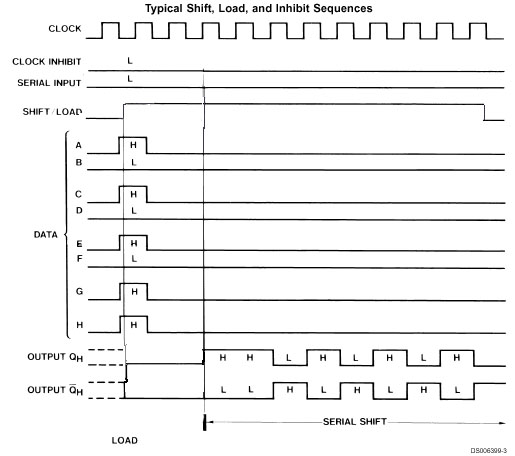
Figure 62 Timing diagram showing improvements
-
- The fix this problem a AND gate will be used so that output of the 74165 goes into one AND input, and a separate circuit will produce a Logic 1 on the other AND input to allow the data to pass though.
- The additional circuit is known as the Inhibit circuit. The inhibit circuit will produce logic 1 for a short duration; just will data is being transmitted. Once the data has been transmitted, the inhibit circuit will produce a logic 0 and prevent any logics from passing though the AND gate.
- In order to accomplish this, a fixed pulse (mono-stable) is required. This can be done using a CD4047BC. This is a Low power Monostable/Astable Multivibrator. It will be used in this particular application as a monostable. By using external resistors and capacitors, this IC can produce required pulses.
- First, we need to know that exact pulse width required. The pulse needs to have a logic 1 to cover the duration when the data is outputted serially. The duration in which the system spends outputting the data is 15.6mS, and is shown below in Figure 63, where an oscilloscope was used to monitor the data.
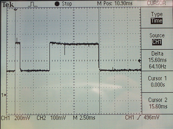
Figure 63 Data to be transmitted , showing period
-
- The monostable will be triggered by the on the 74922, which will go HIGH on a key press.
- A CD4047BC was going to be used, but there was much difficulty using the CD4047BC, as the pulse required was not present, instead there was a high frequency astable signal on the output.
- A 74LS121 timing will now be used to provide the pulse, which is required to produce a logic 1 pulse with a duration greater that 15.6mS.
- The data sheet was used to determine the values of the capacitor and resistor to produce a 15.6mS, although this is less that the specified the components chosen where convenient. This was calculated earlier in the assignment in the Enabling the IR LED section paragraph 9.11 on page 25.
- The circuit was set up, and the pulse was measured to be 16.5mS. Which is very close. There is a slight difference, as the capacitor and resistor has a tolerance.
Enable pulse (from inhibit circuit)
Data
Duration

Figure 64 (Bottom) Data, with (top) LED enable pulse showing period
-
- Before sending the data using infra red, the transmitter and receiver was installed onto separate breadboards, and connected together using one cable, which will be the imaginary IR LINK.
- The circuit was found to function correctly, however the codes displayed on the receiver SSD did not match to the key pressed, hence on the transmitter.
- This was because the keypad used was not correct for the keypad encoder IC.
- In order to solve this problem, a different keypad would be required.
- A second problem found was that the transmitter would not work when two circuit were powered using different power supplies, this problem was cured when both ground was connected together.
- This could be because the data needs to be reference to ground. Although this appears to be a problem, it must be reminded that the end circuit will transmit data using infra red, which will not be sending electrical signal and thus needed to be referenced ground, hence this problem can be temperately solved by connecting both transmitter and receiver grounds together.
- Before the transmitter amplifier is designed and built, the IR LEDs and detectors will be tested to see how far apart they can operate.
- Practical results are shown in paragraph 14 on page 64.
- Next, an amplifier is required to prepare the code to power the IR LED. This will be done using a transistor amplifier circuit.
- The amplifier will be a 741 op-amp
- A 741 amplifier was used, and it was found that stray IR noise was also being amplified, which is a major problem, due to the strength of the noise and hence the signal to noise ratio.
- This will mean that an amplifier cannot be used unless additional circuitry is used to remove the IR noise. This is where the modulation/de-modulation circuitry is required to remove the noise
- A caption of the noise present on the receiver is shown below in Figure 65. The waveform shown is actually the fluorescent lamp switching on and off at 100Hz, thus creating the sinusoidal waveform.
Figure 65 Noise from Fluorescent lights
Ground
DC interference offsetting signal
Figure 66 DC Infra red type interference
-
- The type of interference is shown as a DC which causes in extreme cases, to push the receiver circuitry into saturation. This is also a major problem as unlike the AC noise, the data cannot be superimposed, for the simple reason, the system is already in saturation and will be unable to see the superimposed signal, as it will be cut off.
- All of this noise was to be expected, and a lot of research has been made into preventing this from effecting the project.
- But the cost of the project has exceeded my budget and hence preventing IR noise will be theoretical and not practical.
- The flip-flops were added to the circuit so that each system would remember its status, only change state On or Off, when required, and would otherwise be idle, this was done using flip-flips as memory.
- There are now four LEDs connected to the output of the flip flips, which shows the user whether the system is switched on or off. Problem arose, when some systems would not change state, and hence the circuit was not reliable.
- Measurements where made using a oscilloscope. The data on the receiver was monitored around the controller circuitry. Figure 67 shows a logic pulse from the output of the 74138 (YELLOW) which then goes to an NOT gate, and is shown in Figure 67 at the output of the NOT gate, in BLUE.
- At first there seams no apparent fault.
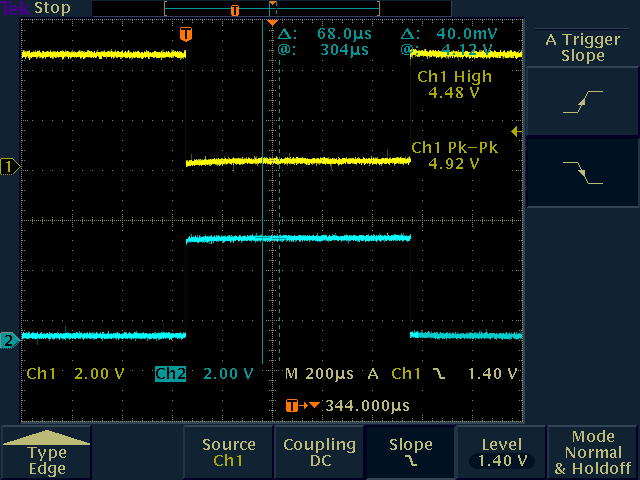
Figure 67 Logic waveform. Zoomed out
-
- After decreasing the time base and monitoring the period in which the logic change state, a potential problem was highlighted, this is shown in Figure 68.
- This caption of the logic pulses, clearly shows that the logic level becomes unstable for a very small period.
- Looking at the YELLOW waveform, it should be a logic high to a logic low. Clearly a the signal goes from a logic high-low-high –low. This will be mistaken as a codes of 1010 and not 10. This causes the system to act erratically, and thus needs to be solved.
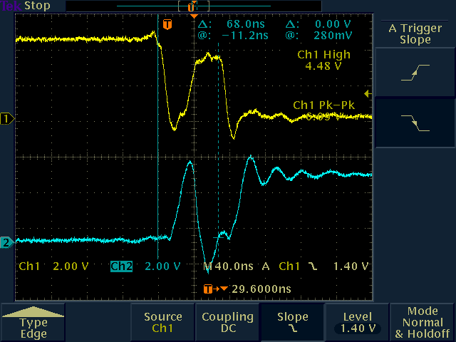
Figure 68 Bounce on Logic switching
-
- This bouncing can be removed by connecting a capacitor from the output of the 74138 (where the data first appears corrupt) with respect to ground.
- Under normal conditioned the DC signals will not pass though the capacitor, as it will appear as a open circuit.
- Any AC signals, such as the bouncing, will pass through the capacitor and thus to ground.
- The periodic time of the bouncing was measured and found to be 29.6nS. This means that at ,, ,
- Although reliable operate was found with a stand 1F Electrolytic capacitor.
- After connecting the capacitors, the signals were measured again and shown in Figure 69.
- Clearly the signal does not have any bouncing. There is a slight ripple but this will have no effect on the systems, as there is no doubt into whether it is a logic 1 or a logic 0.
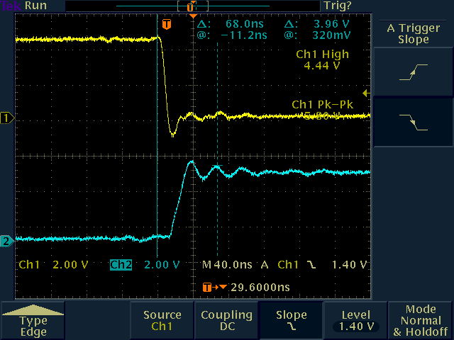
Figure 69 Bouncing removed using capacitors
-
- This problem could have occurred due to the quantity of IC’s in the project, and noise/oscillation could be travelling down the power lines. The capacitor would act as a short circuit to these oscillations, and act as a open circuit to the DC signals.
- Once the receiver was designed, and it was confirmed that the transmitter and the receiver could function together to transmit information, the next stage of the project was to get both the transmitter and the receiver working together at a distance.
- While increasing the distance between the transmitter and the receiver it was noticed that not only was the signal received becoming very small, but the noise also superimposed was increasing.
- The will cause a severe problems with the system as the signal to noise ratio will be very small, hence it will be harder to distinguish between the signal and the noise.
- To overcome this problem the signal to noise ratio will need to be improved. To achieve this the receiver will need to be capable of removing the noise such that the signal is more clear.
- This can be done by modulating the data before it is transmitted and then demodulating the data when it is received. This will remove a high proportion of the noise.
- Due to the complexity of designing a building a modulator and demodulator, this will not be constructed. However, they will be researched.
Filters
-
- This last section has a look as the filters, required to block out some of the noise.
- The following circuit was set up. An IR emitter was used to transmit a stream of DC pulses. A detector was also used to receive the signals

Figure 70 Capturing IR data
-
- The circuit uses the detector as a simple amplifier. With no IR being transmitted, the detector should sense no IR, thus the transistor should remain off. Thus, no current will flow through the collector, emitter to Rload. This will give us 0 volts drop across Rload.
- If some IR was transmitted and sensed by the detector, the transistor would switch on slightly. Thus allowing some current to flow through the resistor Rload, and create a volt drop.
- Since the detector is a linear device, the voltage measured across the resistor Rload, will be directly promotional to the IR being received.
- After setting up the circuit, a small voltage was always apparent across the resistor. The voltage increase when it was aim at a light source. This shows that a filter is required, as IR radiation from light sources will cause unexpected results. For more information on this see paragraph 13.64 on page 60.
- If the detector senses infrared light, the transistor will switch on. Current will then flow through Rload, and will also be a potential difference across Rload, which can be measured
- It was noticed that when the transmitter was switched off, the detector was still showing that IR was being received, as the voltage
- Since there are stray Electromagnetic, these stray signals can become superimposed upon the transmitted signal. This can be a serious program, and the data could become corrupt, and the receiver may be unable to execute the command, or may execute a different command, see paragraph 13.63 on page 60.
- In order to overcome this problem, the signal needs to be filtered before they reach the detector.
- Since the system only uses infrared light, we can use a special coated plastic, which will act as a filter to remove all wavelengths outside the infrared region before reaching the detector.
- The plastic made by Peerless Plastics and Coatings, has a special coating which will only allow wavelengths from 740nm to >1050nm to pass through.
- Looking at the data sheet the filter, copy of particular information shown in Figure 72, will block any wavelengths below 660nm. Between 660nm and 740nm, the filter will let signals pass through, but the transmission percentage will be reduced from 0%-90%.
- Since the operating wavelength is 950nm, the filter will allow the IR data to pass though, and block out unwanted electromagnetic wave from reaching the detector.
- A simple diagram below in Figure 71 illustrates this.
IR Transmitter
Filter
IR receiver
IR data
Ambient light will not pass through filter
Figure 71 Diagram shown set up of IR transmitter and receiver
Operating frequency
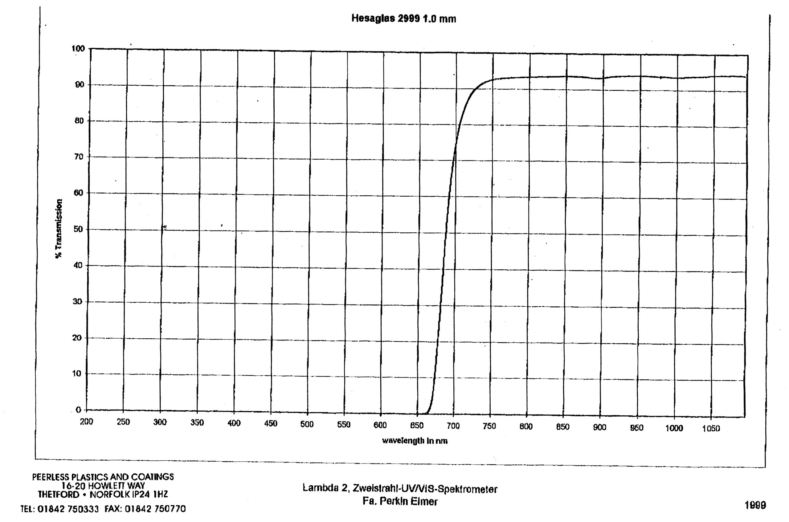
Figure 72 Filter Characteristics
Practical results from the transmitter and receiver
-
- After researching into IR, I decided it would be a good idea to use a emitter and detector to see how increasing the distance in between the transmitter and detector effected the transmission
- This first test was done using sing the SFH313-2 (emitter) and the BVP11 (Detector) the following data was found.
| Distance (mm) | Voltage (V) | Current (mA) |
| 10 | 2.1693 | 2.18 |
| 20 | 2.1518 | 2.17 |
| 50 | 2.12 | 2.1109 |
| 70 | 2.087 | 2.1 |
| 90 | 2.0575 | 2.07 |
| 110 | 1.9656 | 1.98 |
| 150 | 1.31814 | 1.33 |
| 200 | 0.868 | 0.88 |
| 250 | 0.62199 | 0.64 |
| 300 | 0.36211 | 0.38 |
| 400 | 0.2786 | 0.29 |
| 500 | 0.17292 | 0.19 |
| 600 | 0.12564 | 0.15 |
| 700 | 0.089564 | 0.12 |
| 800 | 0.081836 | 0.11 |
| 900 | 0.069569 | 0.09 |
| 1000 | 0.054024 | 0.08 |
| 1100 | 0.048 | 0.07 |
Table 8 Results showing Current/Voltage received against Distance
-
- The data in Table 8, also shown in Figure 73 clearly shows that the Current/Voltage across the detector decreases exponentially with an increase in distance between the transmitter and detector.
- After reading through the data sheets it was found that the BVP11 (Detector) operates on different wavelength to what is specified in the Farnell Catalogue (where the components was purchased from)
- This will mean that there will be a significant reduction in the amount of IR that can be received as looking at the graph in Figure 43 on page 41
- This shows that the spectral sensitivity is not as great when a 950nm wavelength is transmitted. Looking at the graph, it shows a spectral sensitivity of 0.7 which effectively means that it will on receive 30% of the signal which makes it to the detector will be lost.
- In order to improve the amount of IR being received by the detector
- Both transmitter and detector need to operate on the same wavelength
- The detector can be changed for one that is more sensitive
- A more intense IR signal needs to be sent.
- In order to improve the amount of IR received more IR transmitters will be used, which will increase the signal strength, and both transmitter and detector will operate in the same wavelength.
Figure 73 Graph showing Current/Voltage received against Distance
Testing Procedure
-
- Testing procedure is split into two sections, the Transmitter, and Receiver.
Infrared Transmitter
-
-
- Apply 6V to the Transmitter. Measure voltage at the output of the regulator. Verify that the voltage is not greater that 5.25V DC
- Increase voltage to 16V, and verify that the voltage at the output of the regulator is not greater that 5.25V
- Using a oscilloscope check that the signal on the output Infrared LED is sending a signal. The binary codes for each button is shown in Table 9.
-
| Button/System | Binary code |
| 1 | 10000X1 |
| 2 | 10001X1 |
| 3 | 10010 X1 |
| 4 | 10011 X1 |
| 5 | 10100 X1 |
| 6 | 10101 X1 |
| 7 | 10110 X1 |
| 8 | 10111 X1 |
-
-
- Where X is dependent on the position of the Status switch, whether the user wants to switch a system on or off
- Check that each button sends a different code, using the oscilloscope
- Verify that the data transmission is not longer than 16mS
- Verify that the output of the 74121 is greater than 16mS
- Verify that the output of the 555 has a clock with a amplitude of 5V and a frequency of 17.8KHz.
-
Infrared Receiver
-
-
- Apply 6V to the Receiver. Measure voltage at the output of the regulator. Verify that the voltage is not greater that 5.25V DC
- Increase voltage to 16V, and verify that the voltage at the output of the regulator is not greater that 5.25V
- Using a oscilloscope check that the signal on the input Infrared detector is receiving a signal, and it is the same as the signal sent by the transmitter. Amplitude may be attenuated.
- Verify that the output of the 74121 is greater than 16mS
- Verify that the output of the 555 has a clock with a amplitude of 5V and a frequency of 17.8KHz.
-
Researched Improvements on the project
-
-
- Improvements on the project would definitely involve reducing the circuitry on the transmitter and the receiver by using micro controllers.
- The projects can also be improved so it can operate over a larger distance. As mentioned before this can be done by Filters, Encoding & Modulation.
-
Programming a microprocessor.
-
-
- An alternative design to the project, would involve using a microprocessor. A possible microprocessor could be the Intel 8051.
- Two programs would be required. Once for the transmitter and the other for the receiver.
-
The Transmitter
-
-
- The transmitter must be able to allow a user to enter an address and a status code.
- The programmable was actually simulated on a computer, and no REAL ports was actually used, they were viewed using watches. Since we where unable to input data into the microprocessor using ports physically. A hexadecimal code was directed entered into the programming code.
- This is done by using the MOV command. In this case, 81H is loaded into register R0. This code is then outputted to Port 0. This will effectively simulate that a user has physically inputted an 8-bit code into Port 0.
- Next, the software will then look at Port 0 bit 0 and copy this bit to the carry register.
- The program then uses the ACALL command. This will call a subroutine which is indicated by a following address (The address is called ‘DELAY’ is program shown in Table 10).
- In order for the processor to move to the new memory location, it must first remember to current memory location, so that I can return at the end of the subroutine. The ACALL instruction will increment the Program Counter twice in order to get the current 16-bit address. This address will then be pushed into the Stack. The stack pointer is then incremented twice. The program then jumps to the memory location stated in the ACALL command.
- Once the program is within the subroutine, a small delay will be introduced. Since the frequency of transmission will be 17.8KHz, the delay between each bit must be , ,
- In order for the 8051 to create a delay of 56S seconds, it will need to be slowed down. This can be done by decrementing registers through a series of loops.
- Since the Microprocessor runs at 12Mhz, and each of the operations has an oscillation period of 12, this will means that each operation takes 1S. Thus if there is 56 loops, there will be . To create 56 loops you would need two loop, one looping 4 times and the other 14 time, this is hexadecimal number would therefore be is 4 and E.
- Thus, the hexadecimal code required to create 56 loops is shown in the following delay subroutine:
-
| Address | Code | Description |
| Delay | MOV R0,#04H | Load R0 with 04H |
| 80H | MOV R1,#0EH | Load R1 with 0EH |
| 82H | DJNZ R1,$82H | Decrement R2, jump to ADDRESS $82 if not zero |
| 84H | DJNZ R0,$80H | Decrement R1, jump to ADDRESS $80 if not zero |
-
-
- This is done by loading some hexadecimal code into three registers.
- The program will then decrement each of these registers. By calculating the time it takes, and entering in the right hexadecimal code for the register. A 56S delay can be produce.
- The MOV command is then used to move the contains of the carry register to Port 1 bit 0. This will effectively send the bit out in a serially to the receiver though a connecting wire.
- Once the program finishes this delay, the RET command is used. This will POP the HIGH and LOW order bytes of the Program Counter from the stack. The stack will also be decremented by two. This will effectively return from the subroutine.
- The program then continues. The rest of the program follows a similar pattern, except bit 1 of Port 0 is then loaded into the carry register, then bit 2, until bit 7 bit dealt with.
- At this point all 8 bits would have been read and sent serially to port 1 bit 0, and will be transmitted to the receiver.
- The program will then output a series of LOGIC 0’s for its idle state. This is done by loading the carry register with a LOGIC 0, and loading register R0 with AH.
- The program then goes into a loop. This is all done by using the DJNZ command. This command is followed by the Byte to be decremented and the memory location to jump to if the byte is not equal to zero after it has been decremented.
- In each loop the LOGIC 0 in the carry register is moved to Port 1 bit 0, and thus our Logic 0 idle state is created, for 10 loops. If register R0 is not equal to Zero, the program will loop around again, and output another LOGIC 0 to Port 1 bit 0.
- When the R0 does equal Zero, the program will exit the loop and progress through the program.
- The SJMP command is then used, which will is followed by a 16-bit memory location. This command will cause the program to perform an unconditional jump to this memory location, which is 0000H, effectively resetting the transmitter program.
- In practice, the program should wait for the user to enter data into the input port before transmitting the data.
- This can be done by using a loop, in which the program waits for the data to change on Port 0 before continuing.
- The program for the transmitter is shown below in Table 11.
-
| Address | Code | Description |
| 0H | MOV R0,#81H | Load reg R0 with 81H |
| — | MOV P0,R0 | Move reg R0 to Port 0 |
| — | MOV C,P0.0 | Move Port 0 bit 0 to carry |
| — | ACALL DELAY | Call subroutine |
| — | MOV C,P0.1 | Move Port 0 bit 1 to carry |
| — | ACALL DELAY | Call subroutine |
| — | MOV C,P0.2 | Move Port 2 bit 0 to carry |
| — | ACALL DELAY | Call subroutine |
| — | MOV C,P0.3 | Move Port 0 bit 3 to carry |
| — | ACALL DELAY | Call subroutine |
| — | MOV C,P0.4 | Move Port 0 bit 4 to carry |
| — | ACALL DELAY | Call subroutine |
| — | MOV C,P0.5 | Move Port 0 bit 5 to carry |
| — | ACALL DELAY | Call subroutine |
| — | MOV C,P0.6 | Move Port 0 bit 6 to carry |
| — | ACALL DELAY | Call subroutine |
| — | MOV C,P0.7 | Move Port 0 bit 7 to carry |
| — | CLR C | Clear the carry |
| — | MOV R0,#10H | Load R0 with 10H |
| 28H | MOV P1.0,C | Move carry bit to Port 1 bit 0 |
| — | DJNZ R0,$0028H | Decrement R0, jump to ADDRESS if not zero |
| — | SJMP $0000H | Reset program, jump to ADDRESS |
| Delay | MOV R0,#04H | Load R0 with 04H |
| 80H | MOV R1,#0EH | Load R1 with 0EH |
| 82H | DJNZ R1,$82H | Decrement R2, jump to ADDRESS $82 if not zero |
| 84H | DJNZ R0,$80H | Decrement R1, jump to ADDRESS $80 if not zero |
-
-
- Figure 74 shows a flow chart of the Transmitter.
-
Figure 74 Flow chart of Transmitter
The Receiver
-
-
- The receiver needs to capture the serial information from the transmitter and use this information to determine which system to control, and whether the system should be switched ON or OFF.
- The program will work by using Port 0 bit 0 as the input to receiver the bits transmitted. The rest of Port 0 bits will be used as registers, which will be explained later.
- The start of the receiver program will monitor the bits received. Using the MOV command, the bits will be copied to the carry register.
- The program will then use the JC command to check the carry flag to see if it is a logic 1, if this is true it will jump to the 16-bit memory location indicated.
- Under the idle condition, the transmitter will send a series of LOGIC 0’s, this will cause the receiver to loops around, due to the JC command.
- Once the receiver detects a LOGIC 1, the JC command will exit the loop. This is the start bit and will be used to tell the receiver to start capturing the rest of the information transmitted.
- The bit read will then be move to the Carry register. The program will move this bit received to the Most Significant Bit available on Port 0 which will be bit 7, effectively using Port 0 bits as signal bit registers, which will be explained in more depth later.
- The ACALL command is then used to jump to a separate subroutine within the program.
- Within the subroutine a 56S delay will be produce. This is the same as the Transmitter delay.
- Then the next bit on Port 0 bit 0 will be loaded into the C register, this is done using the MOV command.
- The RET command is then used, which will pop the high and low order bytes from the stack, and thus return the program counter to the location just following the ACALL command.
- The program then repeats this process until all of the eight bits have been loaded.
- For example, if the binary code 01010101 was sent to port 0 bit 0, the program will do the following, as shown in Figure 75.
-
Bit 0, (Input for serial data)
Data bit received (Logic 1)
Bit copied to MSB (bit 7)
Next bit of data is now received (logic 0)
It is now copied to the next available MSB (Bit 6)
Next bit of data is now received (logic 1)
It is now copied to the next available MSB (bit 5)
ETC……
Figure 75 Example of storing bit received
-
-
- Once all eight bits have been loaded the program copies the contained of Port 0 as a bytes into register R0.
- Next the status bit is copied from Port 0 bit 5. This is done using the MOV command. Now the receiver knows the address and the status of the system to be controlled.
- The program now uses this information, by comparing the byte now stored in the R0 register, but first we need to know what possible bytes could be stored in the R0 register, which is shown in the following tables.
- There are eight systems, and each system can be switched ON or OFF, two possible combinations. This means there is sixteen different bytes in which to compare as the table below will explain.
-
| System ON | Hexadecimal code | Binary code |
| 0 | 81 | 10000001 |
| 1 | 89 | 10001001 |
| 2 | 91 | 10010001 |
| 3 | 99 | 10011001 |
| 4 | A1 | 10100001 |
| 5 | A9 | 10101001 |
| 6 | B1 | 10110001 |
| 7 | B9 | 10111001 |
Table 12 Codes for each system to be switched ON
| System OFF | Hexadecimal code | Binary code |
| 0 | 85 | 10000101 |
| 1 | 8D | 10001101 |
| 2 | 95 | 10010101 |
| 3 | 9D | 10011101 |
| 4 | A5 | 10100101 |
| 5 | AD | 10101101 |
| 6 | B5 | 10110101 |
| 7 | BD | 10111101 |
Table 13 Codes for each system to be switched OFF
-
-
- The byte stored in the R0 register will now be compared to each of the sixteen possible hex codes mentioned in Table 12, Table 13.
- This is done using the CJME command, which is followed the byte to compare, the hex code in which to compare to the register, and then the memory location to jump to if both hexadecimal codes are different.
- Thus if 81H is loaded into register R0, and the command “CJNE R0,#85H,$0084H”, the program will jump to memory location 0084H.
- This is done sixteen times, until the correct byte is found.
- If 81H is loaded into register R0, and the command is “CJNE R0,#81H,$0084H”, the program will then not jump, but increment the program counter, and run the next command which will output a bit to Port 1.
- This will involve using the MOV command to move the carry bit to the appropriate Port 1 bit location.
- Referring back to Table 12, Table 13. with 81H stored in R0, this represents switching System 0 OFF, and thus will output a logic 0 to Port 1 bit 0.
- Port 1 will be used to show which system is switched ON or OFF. Hence Port 1 bit 0 will represent System 0. If the port bit is Logic High (LED illuminated), then the system is switched ON. If Port 1 bit 7 is a logic 0 (LED not illuminated), this shows that system 7 is switched OFF.
- The program will then continue to the end where the SJMP command is used which will cause a unconditional jump back to 0000H, effectively restarting the program, so that program will once again wait for the start bit from the next byte of data.
- A flow chart is shown over the following pages in Figure 76 and Figure 77.
-
Figure 76 Part one of receiver flow chart
Figure 77 Part two of Receiver flow chat
-
-
- The program for the receiver is shown below in Table 14.
-
| Address | Code | Description |
| 0000H | MOV C,P0.0 | Read port 0 bit 0. Move to carry |
| — | JC $000H | Jump to 0000H if carry=1 |
| — | MOV P0.7,C | Move carry bit to port 0 bit 7 |
| — | ACALL Delay | Call delay |
| — | MOV P0.6,C | Move carry bit to port 0 bit 6 |
| — | ACALL Delay | Call delay |
| — | MOV P0.5,C | Move carry bit to port 0 bit 5 |
| — | ACALL Delay | Call delay |
| — | MOV P0.4,C | Move carry bit to port 0 bit 4 |
| — | ACALL Delay | Call delay |
| — | MOV P0.3,C | Move carry bit to port 0 bit 3 |
| — | ACALL Delay | Call delay |
| — | MOV P0.2,C | Move carry bit to port 0 bit 2 |
| — | ACALL Delay | Call delay |
| — | MOV P0.1,C | Move carry bit to port 0 bit 1 |
| — | ACALL Delay | Call delay |
| — | MOV P0.0,C | Move carry bit to port 0 bit 0 |
| — | ACALL Delay | Call delay |
| — | ||
| — | MOV R0,P0 | Move P0 to Reg R0 |
| MOV C,P0.5 | Move bit 6 to carry | |
| — | ||
| 50H | CJNE R0,#81H,$54H | If reg R0 <> 00H then jump to 54H |
| 52H | MOV P1.0,C | Output carry to Port 1 bit 0 |
| 54H | CJNE R0,#89H,$58H | If reg R0 <> 00H then jump to 58H |
| 56H | MOV P1.0,C | Output carry to Port 1 bit 1 |
| 58H | CJNE R0,#91H,$5CH | If reg R0 <> 00H then jump to 5CH |
| 5AH | MOV P1.0,C | Output carry to Port 1 bit 2 |
| 5CH | CJNE R0,#99H,$60H | If reg R0 <> 00H then jump to 60H |
| 5EH | MOV P1.0,C | Output carry to Port 1 bit 3 |
| 60H | CJNE R0,#R01H,$64H | If reg R0 <> 00H then jump to 64H |
| 62H | MOV P1.0,C | Output carry to Port 1 bit 4 |
| 64H | CJNE R0,#R09H,$68H | If reg R0 <> 00H then jump to 68H |
| 66H | MOV P1.0,C | Output carry to Port 1 bit 5 |
| 68H | CJNE R0,#B1H,$6CH | If reg R0 <> 00H then jump to 6CH |
| 6AH | MOV P1.0,C | Output carry to Port 1 bit 6 |
| 6CH | CJNE R0,#B9H,$72H | If reg R0 <> 00H then jump to 72H |
| 6EH | MOV P1.0,C | Output carry to Port 1 bit 7 |
| 70H | ||
| 72H | CJNE R0,#85H,$76H | If reg R0 <> 00H then jump to 76H |
| 74H | MOV P1.0,C | Output carry to Port 1 bit 0 |
| 76H | CJNE R0,#8DH,$7CH | If reg R0 <> 00H then jump to 7CH |
| 78H | MOV P1.0,C | Output carry to Port 1 bit 1 |
| 7AH | CJNE R0,#95H,$7EH | If reg R0 <> 00H then jump to 7EH |
| 7CH | MOV P1.0,C | Output carry to Port 1 bit 2 |
| 7EH | CJNE R0,#9DH,$82H | If reg R0 <> 00H then jump to 82H |
| 80H | MOV P1.0,C | Output carry to Port 1 bit 3 |
| 82H | CJNE R0,#R05H,$86H | If reg R0 <> 00H then jump to 86H |
| 84H | MOV P1.0,C | Output carry to Port 1 bit 4 |
| 86H | CJNE R0,#R0DH,$8R0H | If reg R0 <> 00H then jump to 8R0H |
| 88H | MOV P1.0,C | Output carry to Port 1 bit 5 |
| 8AH | CJNE R0,#B5H,$8EH | If reg R0 <> 00H then jump to 8EH |
| 8CH | MOV P1.0,C | Output carry to Port 1 bit 6 |
| 8EH | CJNE R0,#BDH,$92H | If reg R0 <> 00H then jump to 92H |
| 90H | MOV P1.0,C | Output carry to Port 1 bit 7 |
| 92H | SJMP $0000H | Reset program, jump to 0000H |
| 94H | (0.1s Delay) | |
| 96H | MOV R0,#04H | Load R0 with 04H |
| 98H | MOV R1,#0EH | Load R1 with 0EH |
| 9AH | DJNZ R1,$9AH | Decrement R2, jump to ADDRESS $9A if not zero |
| 9CH | DJNZ R0,$98H | Decrement R1, jump to ADDRESS $98 if not zero |
| 9EH | RET | Return from subroutine |
Conclusion
-
- At the start of the project I had the task of deciding whether the project should be designed using logic gates, etc or using a single programmable IC to do all the work.
- I decided to design the project using logic gates, as this would make use some of the skills gained on my OND and HNC.
- The project shows the possibilities using logic gates, as they can be used for many applications. The main down fall of this project is the fact that the project is quite cumbersome.
- Measurements shows that the receiver and the transmitter draws over 0.3 amps. This will means that it will NOT last very long on batteries.
- The reason both the transmitter and the receiver draw so much current is due to the shear volume of IC’s running and mainly due to the LEDs being illuminated.
- The LEDs could draw less current by using a larger value resistor in series.
- This method of reducing the current cannot be used however on the IR LEDs as they need plenty of current to produce sufficient illuminence to transmit the IR data.
- Towards the end of my HNC, I have started to develop new skills in programming microprocessors, and now see the potential they could have in my project.
- If the project was redesigned by using a programmable microprocessor such as the Intel 8051, the current drawn would be drastically reduced as the quantity of IC’s used would be reduced. This applies to the transmitter and the receiver.
- Other implications include Cost, Time of manufacture. By using a microprocessor all of the work can be done within the microprocessor by the programme, hence the project would be more reliable as there is less prone to electrical faults.
- Since there is less components the time required to build the project would also be reduced, as mentioned before, the worked would be done by the program, and the program would be simply “Blown/Copied” on to each microprocessor.
- The costs involved would also be reduced, as less labour time would be required to assemble the transmitter and the receiver.
- There would be an increase in cost however to design the program in the first place, but since it can be copied to each microprocessor, the cost in the long run will be cheaper.
- Overall it is clear that using a microprocessor has positive advantages and should be used if the project was to be improved at a later date.
- The aims of the project were to get the transmitter and receiver to operate over a distance of 4 meters. This was not achieved as there was a poor signal to noise ratio.
- As mentioned before this can be solved by using a amplifier and filtering out the noise
- Although Gantt charts were produced, the actual research time and construction time allocated was too small. The project would realistically required two or even three years to properly design a working project to work up the 4meters range as mentioned in the specifications, see paragraph 4.2.1 on page 4.
- However, the knowledge gained during the project has been very useful, and would be very beneficial to any extensions to this project.
- The write up on the project has gone into much depth explaining the potential problems of IR noise, and possible ways in which it can be reduce to improve the performance of the project.
- Since there is no actual encoding or modulation of the data transmitted, the project can be unreliable in bright light, or near sources of strong IR noise.
- However, the project does work very well all things considering, and shows that the transmitter and the receiver do work in harmony together.
Bibliography
| Title | Author | ISBN |
| Digital Systems | Tocci | 0-13-700510-5 |
| Data Sheets | N/A | N/A |
| www.armory.com/~spcecdt/remote/Irremote.html | John H Dubios | N/A |
| www.ee.washington.edu/circuit_archive/text/ir_decode,txt | Juergen Putzger | N/A |
| www.microchip.com | N/A | N/A |
Recent Comments