Summary
- Since I have always had a keen interest in electronic and particularly in Alarm systems, I decided to design and develop a working home alarm system. This alarm system is an updated version of an ‘Bike alarm’ which I designed at school for my GCSE’s.
- The alarm consists of Ultrasonic Transducers to detect any movement near by and Exit and Entry delay timers.
- The alarm system was built successfully. The ultrasonic sensor did detect movement, and the 555 delay timers were a very reliable.
- Thought out the project there has been many problems to deal with. Some of the problems were harder than others. All of the problems that I came across have been overcome.
Introduction
Somerset College Of Arts and Technology commissioned this project.
Since I have always had a keen interest in electronic and particularly in Alarm systems, I decided to design and develop a working home alarm system. This alarm system is an updated version of an ‘Bike alarm’ which I designed at school for my GCSE’s.
Although this project started off with using a remote controller for switching the unit on and off. Later I decided to replace the remote controller with some 555 delay timer circuits as they were simpler to design and more convent for the user of the alarm.
The original idea of using ultrasonic transducers as a sensor did work properly and proved to be highly rewarding as it performed better then expected.
Throughout the project, there were frequent problems to deal with, but the result was a success.
Project Specification
This project consists of the following devices.
- Ultrasonic sensors
The Ultrasonic transmitter uses a 4047 IC to produce an astable signal and an envelope detector and a BRY39 IC to detect any movement.
- 555 Delay timers
The 555 delay timers run in mono-stable mode so that they change state after a period of time. In this case, the timers are set to change state after 30 seconds for the exit delay and 10 seconds for the entry delay.
- Power supply board
The power supply board consists of a 9.1 zener diode for a stabilised power supply of 9 Volts.
Development
Originally, the project was designed to use ultrasonic transducers and a remote control for switching purposes.
The Ultrasonic Transducers
The term Doppler Shift means a shift in frequency. This is the apparent shift in frequency that occurs when energy waves of some form are emitted by a moving object. If the object is moving towards you and waves it sends will appear to be at a higher frequency than they actually are, and if the object is moving away from you there will be an apparent drop in frequency.
An example of this is when a car is moving towards you while sounding it’s horn. There is a sudden large drop in frequency from the horn as the car passes by.
This idea is the basic foundation to the sensors on the alarm.
The signal from the ultrasonic transmitter is sent out and reflected of several walls until it reaches it destination; the ultrasonic receiver. Because the signal can reflect off several walls, it means that it would have a wide coverage.
If an object passes by and reflects the signal towards the ultrasonic receiver then this will cause a shift in frequency (hence doppler shift) on this signal. If the receiver detects more then one-frequency signal, it is designed to operate a relay.
A high gain amplifier is used at the input of the receiver, and the output from this is fed to an envelope detector. If there is only one input signal frequency, the only out from the detector will be a DC bias. If a moving object does cause a shift in frequency of 50Hz in part of the signal, this will produce an audio output of 50Hz from the detector. This is caused by the main signal and the doppler shift signal reacting at the detector to produce a modulated signal.
The output frequency of the envelope detector will depend on the velocity of the object. Normally it would range from a few hundred Hz to a few Hz.
The output from the envelope detector is amplified and then rectified and smoothed to produce a DC signal. This is used to operate a latching relay driver circuit. Under normal conditions, there will be no output from the detector and the relay will not be operated. Virtually any moving object changing the received signal will produce a sufficient AC output from the detector to operate the relay and sound the alarm.
The Ultrasonic Transmitter Circuit
- The transmitting transducer uses a CMOS (Complementary Metal Oxide Semiconductor) 4047 IC (Integrated Circuit) to produce a straightforward astable circuit. This is shown below in Figure 1.
![]()
Figure 1 Circuit diagram of the Ultrasonic Transmitter
L.S1 is an ultrasonic transducer. The reason an ordinary moving coil loudspeaker was not used is because it cannot function very efficiently at ultrasonic frequencies.
The Ultrasonic Transducer which uses the piezoelectric principle and therefore more like a crystal earpiece than a moving coil speaker.
At most frequencies the ultrasonic transducer is not very efficient, but at it’s resonate frequency (40KHz) the efficiency suddenly reaches a pronounced peak.
Information on ultrasonic transmitter circuit
- Adjusting the Pre-set resistor R1 can alter the frequency.
- C2 is a supply decoupling capacitor.
- The transducer is driven from Q and Q. This results in the peak to peak voltage produced across the transducer being almost equal to double the supply rail potential. Since it is first subjected to a positive voltage virtually equal to the supply potential, then a negative voltage almost equal to the supply potential and so on. The peak to peak signal amplitude across the transducer would only be about half of this if the device was to be connected between the negative rail and one of the outputs.
The effects of this would be:
- Weaker signal from the transmitter
- Reduced maximum range
- Lower sensitivity
The Ultrasonic Receiver
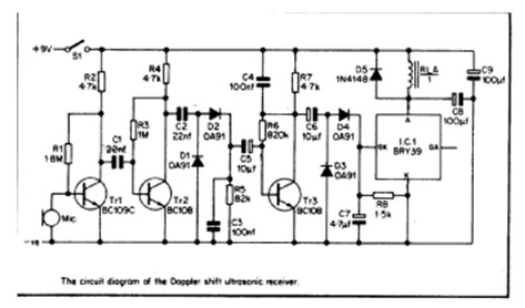
Figure 2 Circuit diagram of the Doppler Shift Ultrasonic Receiver
The microphone is coupled to the input of a straightforward high gain common emitter amplifier which uses TR1. The output from this is coupled to a second command emitter amplifier which is based on TR2. The output from this stage is fed to a simple Envelope Detector circuit which uses D1, D2, C3 and R5. The envelope detector is explained in more detail later.
Any DC produced by the envelope detector is filtered out by C5. The AC signal is fed in to TR4. C4 is used to filter out any of the ultrasonic signal which leaks through to this amplifier and might effect the operation of the receiver.
The output from TR3 is fed to the rectifier and smoothing network which consists of D3, D4 and C7. Normally the Gk terminal of IC 1 is held at the negative supply rail voltage by R8. However, if a Doppler shift occurs, the positive output from the smoothing and rectifier circuit will be sufficient to take this terminal about 0.5 volts positive and IC 1 will be switched on. Once switched on it will remain so, and the relay which forms it’s load will also be switched on.
C8 is needed in order to prevent the circuit from triggering to the on state the moment the supply is connected. D5 is a protective diode and C9 is the only supply decoupling capacitor that is required. S1 is an on/off switch.
The Envelope Detector
The decision making part of the sensor is based in the Envelope Detector.
A basic envelope detector explained below in detail.
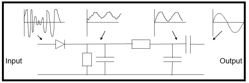
Figure 3 A diagram showing a diode envelope detector.
The main purpose of the diode detector or the Envelope detector is to extract the information (baseband) from the RF (Radio frequency) AM signal.
The first part of the diode detector circuit is basically a ½ wave rectifier. See diagram below, Figure 4
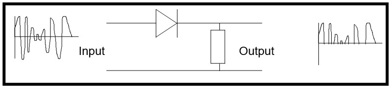
Figure 4 A diagram showing a ½ wave rectifier
However, with the aid of a capacitor in the circuit, the output ripple can be reduce to a (almost) sine wave. Which was transmitted. The values of the resistor and capacitor has to be very accurate, as the CR time will drastically vary the output result. Hence
Figure 5
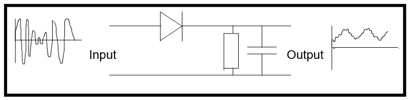
Figure 5 A diagram showing a ½ wave rectifier with capacitor
The next stage consists of a RC (resistive capacitive) filter which can reduce the RF ripple. It also increases the baseband. This is shown below Figure 6.
Figure 6 A diagram showing the RC filter
At the end of the RC filter there is a DC blocking capacitor which removes the DC level.
This is the principle behind the envelope detector.
Accidental Triggering
The only problem now is: “How will the user turn the system on and off without triggering the alarm?”.
There are many solutions to this predicament:
- Remote controller
- Delay timers
- Another sensor to detect when the user has left the room.
The remote controller seamed to be the best solution as it incorporates many electrical principles.
The Remote Controller
Circuit diagrams are shown (below) in Figure 7 ‘The Remote Transmitter’ and (next page) Figure 8 ‘The Remote Receiver’.
![]()
Figure 7 The Remote Transmitter
| Specification | ||
| Receiver | Transmitter | |
| Supply voltage: | 9-12V | |
| Standby current: | 35mA at 12V | |
| Operating current: | 120mA at 12V | 120mA at 12V |
| Carrier frequency: | N/A | 18.5KHz – 23.5KHz |
Table 1 The Specifications for the Remote Controller
After spending many weeks drawing the circuits out on CAD I decided that it was taking up too much time so I started to think of simpler solutions.
Since I had experience in the past with 555 delay circuits. I decided to use these instead of the remote controller.
The 555-timer circuit would work in the following manner.
- As the use switches the system on the first delay circuit of 30 seconds start. This will allow the user 30 seconds to exit the room before the sensor is armed.
- After the 30 seconds has expired the sensor is then armed and waits.
- If someone activates the alarm, the 10-second delay circuit is then activated. This is entry delay timer, so that the user has time to disable the system before the siren starts.
- If the system is not disarmed after the 10 seconds, the siren will then start.
This is explain in a flow chart in Figure 15
The Power Supply
The power supply needs to supply a constant 9 volts while the load is changing (due to timer switching on and off).
I first thought of using a potential divider to produce 9 volts, see Figure 9 below.
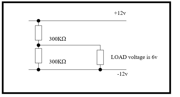
Figure 9 Circuit diagram of a potential divider
Although this circuit did supply the correct voltage for a single load. Once I added more loads the voltage levels drop. This was a big problem.
I then thought if I had multiple potential dividers, the circuit would be more stable. This also failed.
I then started to find alternative way to provide a stabilised power supply. Then is when I came across the zener diode circuit. See Figure 10.
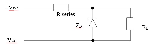
Figure 10 A diagram of a zener diode circuit
The reverse characteristics of a zener diode working in the breakdown region shows that the voltage is virtually constant for a wide range of current. This means if the load current (IL) should increase the current through the zener diode (ID) should decrease and a constant voltage drop across Rs will be maintained. This means the output voltage of VL will also be constant.
This also applies if the load current should decrease.
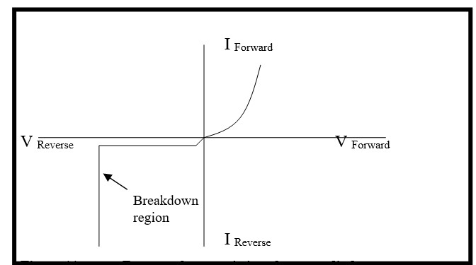
Figure 11 Reverse characteristics of a zener diode
In order for the circuit to operate as a voltage stabiliser, the zener diode must operate in the breakdown region. The value of the series resistor (RS) and the load must be such that the potential difference across the diode forces the diode in the breakdown region.
The delay timers consist of an 555 timer chip running in a monostable mode.
The timing of the circuit was calculated using the formula shown below in Equation 1
Time=1.1 x Capacitance x Resistance
Equation 1 The delay formula for a 555 timer
To calculate the 10 second and 30-second delay timers I use the following method.
T=1.1CR
27=1.1 x (33 x 10-6) x (746 x 103) seconds
So, C = 33F, R = 746K
21=1.1 x (100 x 10-6) x (100 x 103) seconds
So C = 100F, R = 100K
I did notice that the calculated and measured values where not exactly the same. This was due to the tolerance in the components hence resisters and capacitors.
Results
Once the project was completed, I started to test the system out. I found that the 555-delay circuits were very adequate for the job in hand so I quite pleased that I used these times instead of the remote controller.
The ultrasonic sensor works perfectly. Although the object has to be move at a far pace in order to be detected, the principle behind the unit is functioning as expected.
I did find that from 1 inch – 8 inches the sensors were fine and that the receiver is more sensitive when closer to the transmitter and the decreases in sensitivity when move apart. This could be because the signal is not strong enough to propagate through the air (due to the attenuation) or/and the receiver is not sensitive enough to pick up the weak signals.
The sensors were tested at several intervals and did detect movement while the ultrasonic transducers were 8 inches apart in ‘line of sight’ (hence directly facing each other).
The sensors also worked very well when aimed at a still object at an angle (as shown in Figure 12). This would mean that the sensors would cover a wider area then if they were placed in ‘line of sight’.
The 555-timer delay circuit was very reliable. I did find that the time delay was not what the formula predicted. This could be due to the tolerance in the components.
Conclusion
Thought out the project there has been many problems to deal with. Some of the problems were harder than others. All of the problems that I came across have been overcome.
Seeing the finished project shows that I do have the technical knowledge in electronics.
Future improvements
- There could be some LED’s to show the user what is happening. Hence, when each circuit is running an LED could turn on.
- A LCD displace could be used to show a visual countdown on the delay timers
- More sensors could be used. The can be done using a muitplexer and a microprocessor to check each sensor.
Appendix
The Bipolar Transistor
The bipolar transistor is a small chip of semiconductor, ordinarily silicon or germanium, with an internal structure resembling two back-to-back junction diodes. This structure is achieved by transforming both ends of a bar of n-type semiconductor into p-type material. The result is a pair of pn junctions within a single semiconductor chip, and the transistor is called a pnp device. A second way to achieve the desired pair of junctions is to transform both ends of a p-type bar into n-type material to give a npn device.
Whether pnp or npn, the central region of the transistor, which is called the base, controls the current flowing between the two outer regions, which are called the emitter and collector.
Operation.
In the operation of, for example, the npn transistor, electrons from an external source are injected into the emitter, where they readily cross over into the p-type base. The holes (“missing” electrons) in the base are quickly filled by the incoming electrons, and the resulting negative charge acts to repel further electrons that would otherwise arrive from the emitter.
A comparatively small positive current applied to the base can produce additional holes that will, in turn, permit more electrons to be injected into the base from the emitter. The base region purposefully contains significantly fewer holes than the emitter and collector contain free electrons, so a substantial percentage of the injected electrons pass through the base and enter the collector before the holes in the base are filled. The application of additional holes into the base encourages more or less emitter-collector current flow, much as a throttle controls the speed of an engine.
Emitter current passes from the base to the collector even though the base is more positive than the collector (reverse bias). If the base-collector junction were fabricated like the pn junction in a conventional diode, only a tiny reverse current would flow.
In a transistor, however, the base is lightly doped and exceedingly thin. The light dopant concentration means many electrons must enter the base before all the holes are filled, and the thin geometry means many electrons are immediately adjacent to the base-collector junction. Consequently, as many as 99% of the free electrons injected into the base wander into the base-collector junction region and are swept into the collector.
Applications.
Because the emitter-collector current is up to several hundred times greater than the emitter-base current, the transistor qualifies as an efficient current amplifier. In a typical application, a small current generated by a voice directed toward a microphone is applied to the base of a transistor. This small base current controls the much larger emitter-collector current that is applied to the terminals of a loudspeaker, which emits a greatly amplified sound.
A junction transistor may also be used as an electronic switch. Below a point known as saturation, or cut-off, the ratio of the base current to the emitter-collector current is constant. At saturation the transistor reaches its highest possible conductivity, and further increases in base current fail to increase the emitter-collector current. A comparatively small base current easily saturates a transistor into full conduction and causes it to act as a solid-state on-off switch. This mode of operation has many uses, particularly in digital electronic circuits.
Virtually identical action occurs in pnp units, the single exception being that holes rather than electrons are the principal carriers of current. Consequently, the polarity of current applied to a pnp transistor is opposite that applied to a npn device. Both types are used equally in electronic circuits.
New Developments
Complementary metal-oxide-semiconductor circuitry, or CMOS, comprises pairs of n- and p-channel transistors that are controlled at the same time by a single circuit. This makes more efficient use of the chip and cuts down on both power need and heat production. For these reasons, CMOS technology is gaining wide acceptance despite its slower operating speeds. Emitted coupling logic, ECL, is a bipolar technology that is extremely fast but also expensive and not compatible with other technologies. Other areas of research include the development of gallium-arsenide chips, superconducting materials, and electron tunneling through junctions
Capacitor
A capacitor is an electrical component that consists of two conductors separated by an insulator; it has the property of CAPACITANCE and so opposes any change in the voltage across its terminals. Formerly known as a condenser, the capacitor is the only device other than a BATTERY that can store electrical energy, and it is this stored energy that enables the capacitor to resist changes of voltage. The capacitance of a capacitor–its ability to store electric CHARGE (and energy)–is measured in units of farads (F) and fractions of a farad: microfarads and picofarads (pF).
The earliest form of capacitor was the LEYDEN JAR, invented in the 18th century to study electrical phenomena. It was essentially a glass jar with inside and outside layers of metal foil. Modern capacitors are less cumbersome. The simplest capacitor consists of two metal plates separated by an insulator, or DIELECTRIC. The larger the plate area and the smaller the separation, the larger will be the capacitance. The characteristics and applications of capacitors also depend upon the dielectric used. Common materials include paper, mica, ceramic, plastic, electrolytes, and air.
Capacitors can be described in terms of their capacitance, their maximum DC (direct current) working voltage (DCWV), the type of dielectric, and whether the value of the capacitance is fixed or variable.
Because the dielectric is an insulator, a capacitor will not permit a direct current to flow through it, but its continuous charging and discharging action will allow ALTERNATING CURRENT (AC) to pass. Thus, one of the important applications of capacitors is to block DC, but pass, or couple, AC from one amplifier to another; such capacitors are known as blocking, or coupling, capacitors. Inexpensive paper capacitors used for this purpose are produced by interleaving two sheets of aluminium foil and two sheets of paper and rolling them into a tubular form.
Ceramic capacitors, consisting of a ceramic disk between two metal films, are similar to the paper type; but they have larger capacitance’s (1 picofarad-0.1 microfarad), are smaller in size, and work at voltages up to 1,000 V. Mica capacitors have values of capacitance similar to the ceramic type, but they can be used at voltages as high as 35,000 V and frequencies as high as 10,000 MHz.
Plastic film capacitors use polystyrene as a dielectric. More expensive than the paper capacitor, this type is smaller, has very high insulation resistance, and has capacitance ranging from 5 pF to 0.47 microfarad.
Many applications in electronics require electrolytic capacitors, which are relatively small in size but have very high values of capacitance because of the very thin dielectric used to separate the plates. A disadvantage of an electrolytic capacitor is its high leakage current (the current that flows across the plates). Electrolytic capacitors are used as electronic filters, in power supplies that rectify AC (convert AC to DC). The rectified output still contains some AC, so a large capacitor is often connected across the output. Energy stored by the capacitor when the voltage is increasing is released to the load when the voltage is decreasing, which helps to smooth out the flow of energy.
Electrolytic capacitors are also used in electronic photographic flash units. A capacitor having a capacitance of a few hundred microfarads is allowed to charge from a battery pack for several seconds. All of this energy is then used to light a bulb for a short time, producing a bright flash of light.
Capacitors are commonly used in conventional ignition systems to reduce arcing across the points. Variable capacitors consist of two interleaved sets of metal plates, one set fixed and one movable; the air surrounding the plates serves as the dielectric. Such capacitors are used in radio tuners.
Resistor
A resistor is an electrical component that has the property of resistance, which enables it to oppose the flow of current in a circuit.
This electrical resistance, caused by the collisions of electrons in motion, is responsible for converting electrical energy into some other form, such as
- Heat
- Light
In electronic circuits, however, resistors are introduced into a circuit to:
- Limit current to a safe value
- Drop voltage to a required value
- Divide voltage from a single source into fractions of that value
- Discharge energy as from a CAPACITOR.
Resistors are usually described in terms of:
- Their electrical resistance, in ohms (represented by the Greek upper-case letter omega)
- Their ability to dissipate heat, in watts (W)
- Their construction (composition, wirewound, or film)
- Their functional makeup (fixed or variable)
- The percentage tolerance of their resistive value.
Fixed-carbon-composition resistors are available in standard values from 2 ohms to 30 megohms or 30 million ohms, in power ratings from 1&10 W to 2 W. Their values are indicated by a series of standard colour-coded stripes painted on a bakelite case that is moulded over the graphite interior.
Power-type resistors consist of an alloy ribbon, such as nickel-chromium-iron, wrapped around a ceramic support to form a wirewound resistor capable of dissipating hundreds of watts. A film-type resistor is composed of a resistive film of carbon or metal deposited on an insulating cylinder. It is used for high-frequency and high-voltage applications.
Variable resistors may be either composition type or wirewound. They have a sliding contact, so that the amount of resistance can be varied. Low-powered types (three-terminal devices) are called POTENTIOMETERS and are used for volume controls in radios and amplifiers. High-powered types called RHEOSTATS have only two terminals and may be used, for example, in light-dimming switches
Diode
A diode is an electronic device with two terminals that allows a current through it in only one direction, depending on the polarity of the voltage connected across it. A diode may be either an ELECTRON TUBE or a SEMICONDUCTOR device.
Operation
The electron-tube diode uses a heated cathode to emit electrons. Since the electrons have a negative charge, they will move through the vacuum to the anode if the anode is positive. This flow of electrons constitutes a current and will take place whenever the anode is positive with respect to the cathode. If the anode is negative, the electrons will not move through the tube, and there will be no current. Thus, the diode is a device that is sensitive to polarity. If an alternating voltage–one whose polarity reverses regularly–is connected across the diode, there will be a current through the diode for only half of each cycle, that is, only when the applied voltage makes the anode positive with respect to the cathode. This process, converting AC to DC, is known as rectification and is performed by a device called a RECTIFIER. Rectification is the single most important application for diodes.
A semiconductor diode, typically made from silicon, is very small (approximately a 3-mm/0.12-in cube), compared with a tube that is 3 cm (1.2 in) in diameter and 7 cm (2.8 in) long. No heat is required for its operation, and it is much more rugged than a tube. Basically, the solid-state diode consists of pure silicon with each end modified by the addition of some “impurity” material.
This arrangement produces a P-type anode, in which holes, or positive charges, are available to conduct current, and an N-type cathode, in which free electrons supply conduction. The area at which the P- and N-types meet is called a PN junction. If this junction is forward biased, by connecting a positive voltage to the anode (P-type) and the negative voltage to the N-type, then holes and electrons can cross the junction and produce a current. If the opposite voltage is applied–a condition of reverse bias–the holes and electrons are both drawn away from the junction, and there is no current.
Applications
If a single diode is connected in series with an AC supply voltage and a load, such as a battery to be recharged or a DC motor, half-wave rectification results. If two diodes are used with a centre-tapped transformer or if four diodes are used in a bridge-type rectifier, full-wave rectification is obtained. In this case, the current drops to zero only momentarily each half cycle. By using a device called a FILTER, this current may be smoothed to give a more steady value of DC. This constitutes a DC power supply. It is used to power transistors or tubes in electronic equipment, such as radios, televisions, and amplifiers that operate from the 60-Hz AC supply voltage.
One precaution that must be observed in rectification concerns the maximum reverse voltage or peak inverse voltage (PIV) that occurs across the diode when it is not conducting. If this rating of the diode is exceeded, the diode will break down and current will flow in the reverse direction. If this occurs, the device may be damaged because of excessive heat. However, a ZENER DIODE is specifically constructed so that it will break down abruptly at some accurately known voltage. If the current is limited to some safe value, the voltage across the diode is constant, independent of the current through the diode. This characteristic is used in a VOLTAGE REGULATOR to maintain a voltage from a power supply at some relatively constant value even though the load current may vary widely.
Transformer
A transformer is an electrical device that transfers electric energy from one coil, or winding, to another by electromagnetic induction. The transferred energy may be at a higher or lower voltage. Transformers can only operate on alternating current (AC) or on direct current with a superimposed AC component (pulsating DC).
Transformers are generally classed as step-up or step-down transformers. A step-up transformer increases the voltage, and a step-down transformer reduces it. At electric generating plants, step-up transformers (called generator transformers) increase the generator voltage to a higher voltage, which is then transmitted through power lines over long distances with little loss.
In the locality where the electricity will be used, step-down transformers then lower the voltage. A distribution transformer makes the final step-down in voltage for homes and businesses. Consumers may use additional step-down transformers to operate such devices as doorbells and toy electric trains.
Operation
The operation of the transformer is based on the principle discovered in 1830 by Joseph Henry that electrical energy can be transferred efficiently by mutual ELECTROMAGNETIC INDUCTION from one winding to another.
When the primary winding is energised by an AC source, an alternating magnetic flux is established in the transformer core. This flux links the turns of both primary and secondary, thereby inducing voltages in them. Because the same flux cuts both windings, the same voltage is induced in each turn of both windings.
The total induced voltage in each winding is therefore proportional to the number of turns in that winding. This proportion is known as the turns ratio, which, when multiplied by the applied voltage, determines the secondary voltage.
Transformers have no moving parts. The typical transformer has two windings, insulated electrically from each other, wound on a common magnetic circuit of laminated sheet steel (the core). The core provides a circuit of low reluctance for the magnetic flux, or lines of force. The primary is always connected to the source of power, and the secondary winding receives the electrical energy by mutual induction from the primary winding and delivers it to the connected electric load. In some transformer windings, taps are provided so that less than the full number of turns may be used. This allows a transformer with a single pair of coils to provide more than one voltage or current.
Two types of transformer construction are the core type and the shell type. In the core-type transformer, the windings surround the laminated metal core. In the shell-type transformer, the metal core surrounds the windings. Distribution transformers are generally of the core type, whereas some of the largest high-voltage power transformers are of the shell type. Small transformers are air cooled, and larger transformers usually are oil cooled.
Transformers are built in single-phase and polyphase units. Most power and distribution systems use three-phase lines. A three-phase transformer consists of separate insulated windings for the different phases. The windings are wound on a three-legged core capable of establishing three magnetic fluxes displaced by 120 deg in time phase. Transformers also may be classed according to the frequency range for which they are designed, such as audio frequency, power frequency, and radio frequency. Regardless of type, however, all transformers operate on the same basic principles.
Transformers require little care and maintenance because of their simple, rugged, and durable construction. The efficiency of transformers is high. In some transformers efficiency is 99 percent. Because of this efficiency and their ability to vary voltage easily, transformers are largely responsible for the more extensive use of alternating current than direct current
Amplitude Modulation
In radio-telephone communication or standard broadcast transmissions the speech and music are used to modulate the carrier. This process means that the intelligence to be transmitted is used to vary some property of the carrier. One method is to superimpose the intelligence on the carrier by varying the amplitude of the carrier, hence the term amplitude modulation (AM). The modulating audio signal (speech or music) is applied to a MICROPHONE. This produces electrical signals that alternate, positively and negatively. After amplification, these signals are applied to a modulator. When the audio signals go positive, they increase the amplitude of the carrier; when they go negative, they decrease the amplitude of the carrier. The amplitude of the carrier now has superimposed on it the variation of the audio signal, with peaks and valleys dependent on the volume of the audio input to the microphone. The carrier has been modulated and, after further amplification, is sent by means of a transmission line to the transmitting antenna.
The maximum modulating frequency permitted by AM broadcast stations is 5 kHz at carrier frequencies between 535 and 1,605 kHz. The strongest AM stations have a power output of 50,000 watts.
Relay
A relay is essentially an electrically controlled SWITCH that is used to open or close an electric circuit. The switch can be actuated by various means. Electromechanical operation is the most common and will be emphasised below, but other types of actuation are possible. An electromechanical device produces mechanical motion when it is energised by an electric current. A SOLENOID is such a device, and solenoids are often used in relays.
A standard type of relay consists of a coil with an enclosed, fixed iron core and a nearby movable armature. When the coil is energised, the armature is attracted to it; the resulting motion is then used to open or close the relay circuit. Such a relay requires a power of several watts for proper operation.
Zener Diode
A Zener diode is a semiconductor component, named for the American physicist Clarence Zener, that functions as a VOLTAGE REGULATOR. When current is passed through the device in the forward direction it behaves much like any other semiconductor diode.
When current is passed through the device in the reverse direction, the normally high reverse resistance suddenly becomes very low when the applied voltage exceeds a specified minimum level called the Zener breakdown voltage, which can be selected to be from about three volts to hundreds of volts. This characteristic has the effect of regulating the applied voltage to the level of the Zener breakdown voltage. Zener diodes are commonly used to protect sensitive electronic circuits and components from excess voltage
Switch
Mechanical and electronic switches are devices used to interrupt or re-establish the flow of electricity in a circuit. When the switch performs automatically under prescribed conditions, it is called a CIRCUIT BREAKER. A mechanical switch operates by joining and separating electrical contacts at some point in the circuit. A drawback of such a switch is that when it is opened, it induces a spark (arcing), which creates high temperatures that can damage the switch. There are various methods for preventing arcing or, at least, extinguishing the arc rapidly after it occurs.
On developing the alarm system many problems were encountered.
- On 6-11-97 I found differculty deciding how the system should be activated and de-activated.
The main choices where using a 555 timer and a remote controller. The remote controller would give the user more control of the system but add unnecessary complications.
After mush consideration I felt I necessary to use a number of 555 timers as they are easy to develop and very reliable.
- 27-11-97
To work out the time delays for the 555 timer circuits the formula T = 1.1CR was used. I felt it necessary to check the circuit on a breadboard to see if the calculation would give the correct values for the capacitor and resistors.
Once the circuit was constructed on the breadboard, I found that the time delays were out by about 2-10 seconds. I believe it was due to the resistance of the breadboard and the (long) wires to connect the components. A PCB was then designed and tested. The timing now seamed to be much more accurate.
- On the 23-2-98 the ultrasonic transmitter & receiver was constructed I then began to test them.
Once the variable resistor was adjusted to maximum output (which occurs at 40KHz, resonance frequency) I was able to see the transmitted signal on the transmitter and receiver. I first noticed a problem when the signal was not being processed in the receiving circuit. I later found some design faults on the ultrasonic receiving board and attempted to redesign and construct it.
- 23-2-98
The ultrasonic receiver was rebuilt but a one design fault was not noticed. There was no power connected to the board. Drilling two holes in the appropriate places easily solved this.
- On the 27-3-98 I made the decided to make the following modifications to the circuits
555 timer circuits
- After looking through the 555 timer specifications I found that the timer could source enough current for the ultrasonic input relay. This means that I can now remove the transistor out of the delay circuit.
- During the developing stages I forgot that the 555-timer circuit needs a closed circuit then an open circuit on the trigger pin. Because the jumper only provides a closed circuit the monostable mode never starts hence it never starts a delay. To solve this problem a capacitor was placed in series with the jumper so That it would act as an open circuit while it was charging up.
- Improve text. A) Line up text properly. B) Name the jumpers.
- Put insulation around the connection join from the wire to the transmitter
Ultrasonic receiver
- Put a diode in between the power points of the input relay. This will prevent a back emf from the coil damaging any components while it changes states.
- Since there have been some modifications to the 555 timer circuit it means that the ultrasonic receiver will also need some alterations. This will include making the input relay normally closed. This way the 555 timer will send a voltage to the input relay to make it open for 30 seconds.
- Since the power point were placed incorrectly (in parallel), this time they will be changed to be in series.
- Improve text. A)Line up text properly. B)Name the relays.
- Put insulation around the connection join from the wire to the receiver.
Power Supply
- Change the Power supply board so that the pads are larger.
- Line the text on board properly.
Siren power supply
- Add some pads so that a relay can be used.
- Line the text on the board properly.
- On the 7-4-98 I tested the new boards, but they did not function properly. The timer would not switch off the relay and the ultrasonic receiver would not work properly.
The fault with the delay circuit was that they needed another diode to prevent ant back e.m.f.
The fault on the ultra sonic receiver circuits was not found. This was mainly because I do not have the necessary testing equipment available at home.
I did find some tracks were joined together when they should not have been. This was due to some bad development on the boards.
I did notice that the output relay was incorrectly labelled, the normally closed and normally open was the wrong way round. This caused the 10-second delay circuit to start operating preminturly.
The resistor on the power supply circuit was over heating. This only occurs when a large supply of current is necessary hence three or more circuit on. This component may need some kind of heat sink or a higher wattage rating.
Recent Comments